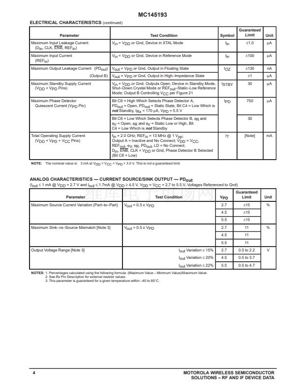
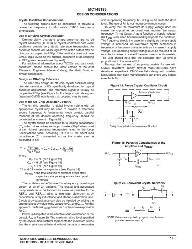
to 10 k鈩?must be used. Parameters to consider when sizing
rate.
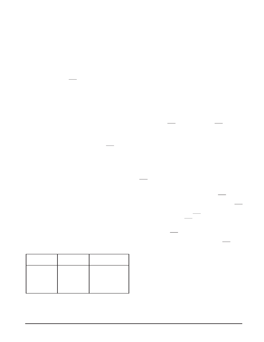
Table 3. Register Access
鈮?/div>
32
Values > 32
Accessed
Register
C Register
R Register
A Register
Not Allowed
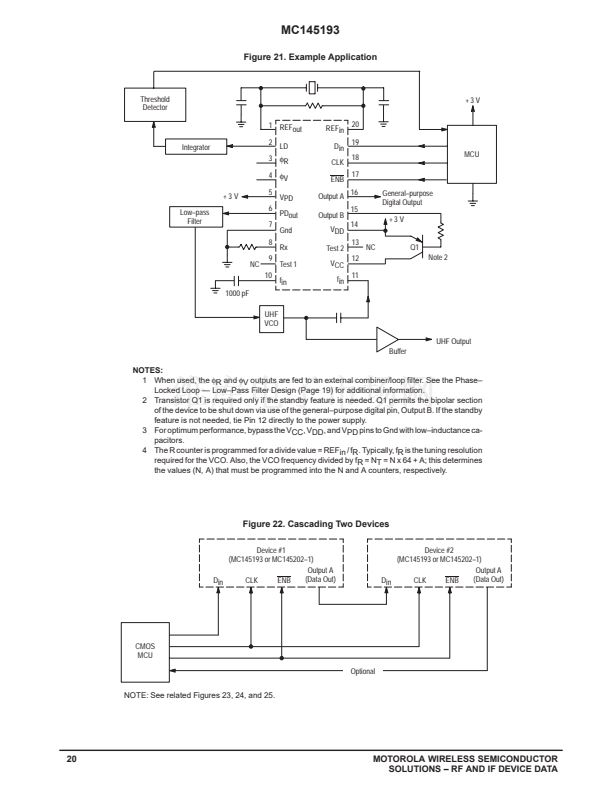
See Figures
22 鈥?25
Bit
Nomenclature
C7, C6, C5, . . ., C0
R15, R14, R13, . . ., R0
A23, A22, A21, . . ., A0
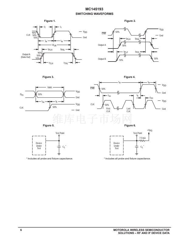
CLK
Serial Data Clock Input (Pin 18)
Low鈥搕o鈥揾igh transitions on CLK shift bits available at the
Din pin, while high鈥搕o鈥搇ow transitions shift bits from Output A
(when configured as Data Out, see Pin 16). The
24鈥?/2鈥搒tage shift register is static, allowing clock rates
down to dc in a continuous or intermittent mode.
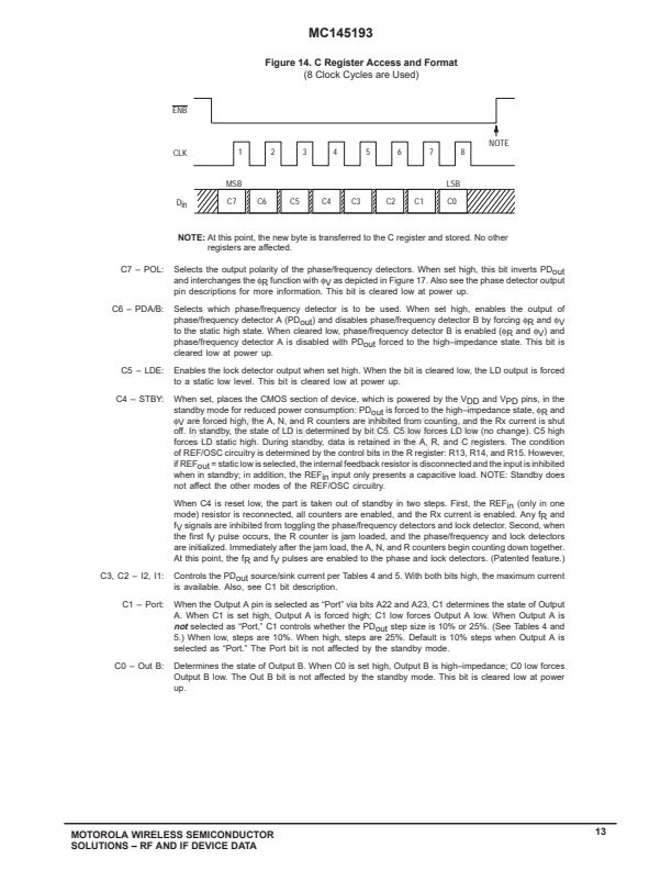
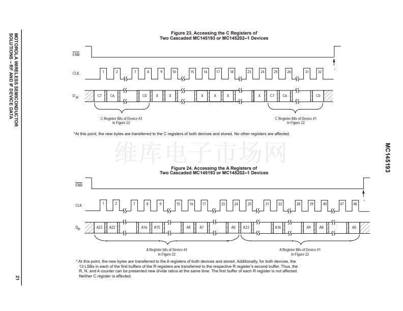
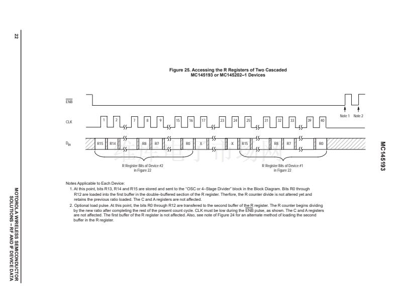
Eight clock cycles are required to access the C register.
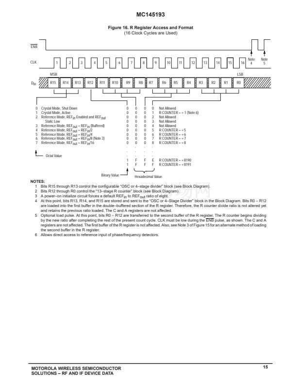
Sixteen clock cycles are needed for the first buffer of the R
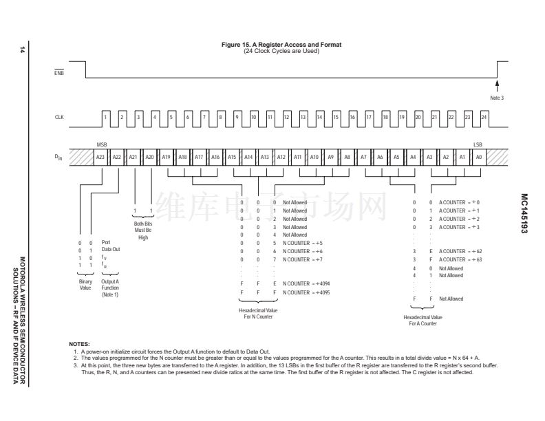
register. Twenty鈥揻our cycles are used to access the A
register. See Table 3 and Figures 14, 15, and 16. The number
of clocks required for cascaded devices is shown in Figures
23 through 25.
CLK typically switches near 50% of VDD and has a
Schmitt鈥搕riggered input buffer. Slow CLK rise and fall times
are allowed. See the last paragraph of
Din
for more
information.
NOTE
To guarantee proper operation of the power鈥搊n
reset (POR) circuit, the CLK pin must be held at
Gnd (with ENB being a don鈥檛 care) or ENB must
be held at the potential of the V+ pin (with CLK
being a don鈥檛 care) during power鈥搖p. Floating,
toggling, or having these pins in the wrong state
during power鈥搖p does not harm the chip, but
causes two potentially undesirable effects. First,
the outputs of the device power up in an unknown
state. Second, if two devices are cascaded, the A
Registers must be written twice after power up.
After these two accesses, the two cascaded chips
perform normally.
ENB
Active Low Enable Input (Pin 17)
This pin is used to activate the serial interface to allow the
transfer of data to/from the device. When ENB is in an
inactive high state, shifting is inhibited and the port is held in
the initialized state. To transfer data to the device, ENB
(which must start inactive high) is taken low, a serial transfer
is made via Din and CLK, and ENB is taken back high. The
low鈥搕o鈥揾igh transition on ENB transfers data to the C or A
registers and first buffer of the R register, depending on the
data stream length per Table 3.
Transitions on ENB must not be attempted while CLK is
high. This puts the device out of synchronization with the
microcontroller. Resynchronization occurs when ENB is high
and CLK is low.
This input is also Schmitt鈥搕riggered and switches near
50% of VDD, thereby minimizing the chance of loading
erroneous data into the registers. See the last paragraph of
Din
for more information.
For POR information, see the note for the
CLK pin.
MOTOROLA WIRELESS SEMICONDUCTOR
SOLUTIONS 鈥?RF AND IF DEVICE DATA
9


 1
1
 2
2
 3
3
 4
4
 5
5
 6
6
 7
7
 8
8
 9
9
 10
10
 11
11
 12
12
 13
13
 14
14
 15
15
 16
16
 17
17
 18
18
 19
19
 20
20
 21
21
 22
22
 23
23
 24
24
