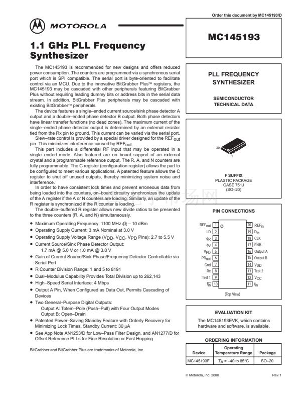
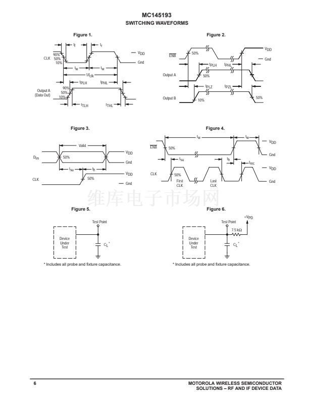
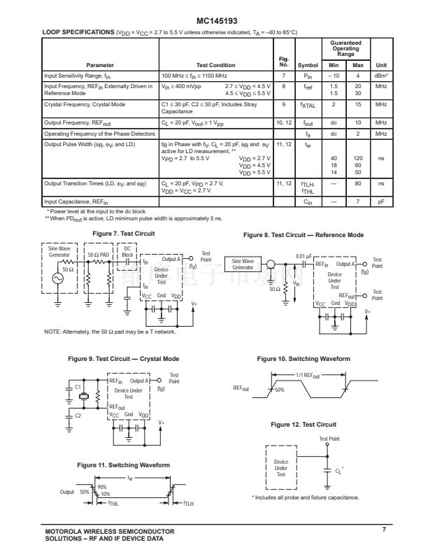
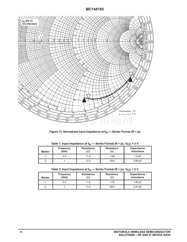
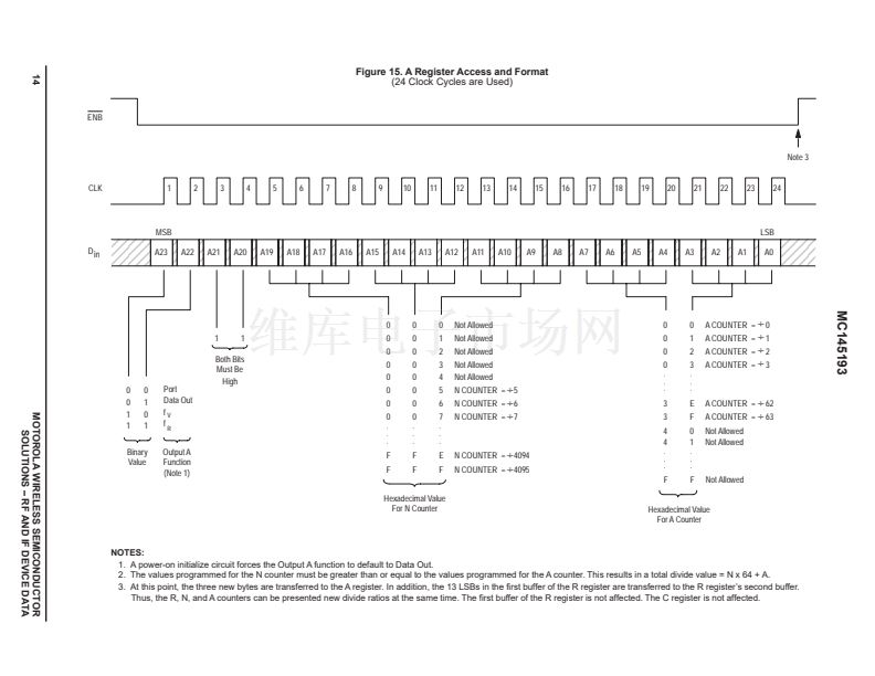
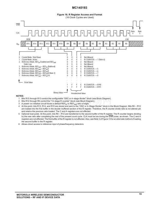
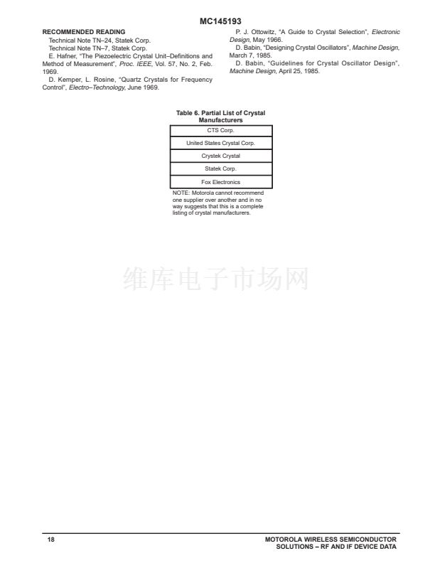
MC145193
TEST POINT PINS
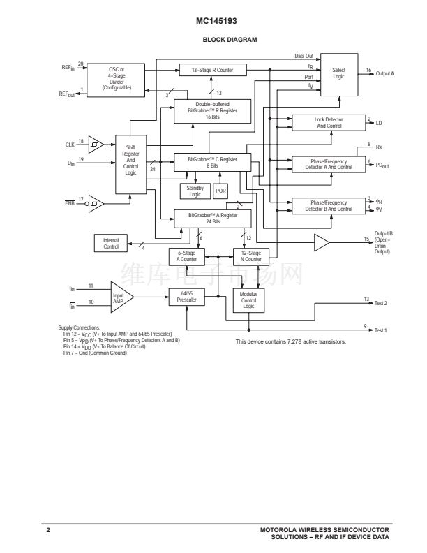
Test 1
Modulus Control Signal (Pin 9)
This pin may be used in conjunction with the Test 2 pin for
access to the on鈥揵oard 64/65 prescaler. When Test 1 is low,
the prescaler divides by 65. When high, the prescaler divides
by 64.
CAUTION
This pin is an unbuffered output and must be
floated in an actual application. This pin must be
attached to an isolated pad with no trace.
Test 2
Prescaler Output (Pin 13)
This pin may be used to access the on鈥揵oard 64/65
prescaler output.
CAUTION
This pin is an unbuffered output and must be
floated in an actual application. This pin must be
attached to an isolated pad with no trace.
POWER SUPPLY PINS
VDD
Positive Power Supply (Pin 14)
This pin supplies power to the main CMOS digital portion
of the device. Also, this pin, in conjunction with the Rx
resistor, determines the internal reference current for the
PDout pin. The voltage range is 2.7 to 5.5 V with respect to
the Gnd pin.
For optimum performance, VDD should be bypassed to
Gnd using a low鈥搃nductance capacitor mounted very close to
these pins. Lead lengths on the capacitor should be
minimized.
VCC
Positive Power Supply (Pin 12)
This pin supplies power to the RF amp and 64/65
prescaler. The voltage range is 2.7 to 5.5 V with respect to
the Gnd pin. In standby mode, the VCC pin still draws a few
milliamps from the power supply. This current drain can be
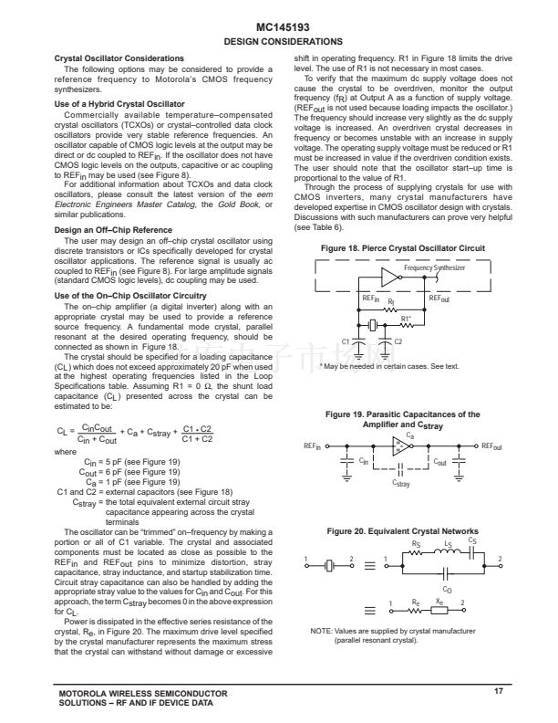
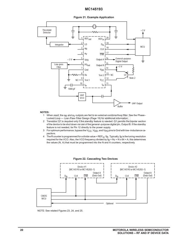
eliminated with the use of transistor Q1 as shown in
Figure 21.
For optimum performance, VCC should be bypassed to
Gnd using a low鈥搃nductance capacitor mounted very close to
these pins. Lead lengths on the capacitor should be
minimized.
VPD
Positive Power Supply (Pin 5)
This pin supplies power to both phase/frequency detectors
A and B. The voltage applied on this pin may be more or less
than the potential applied to the VDD and VCC pins. The
voltage range for VPD is 2.7 to 5.5 V with respect to the Gnd
pin.
For optimum performance, VPD should be bypassed to
Gnd using a low鈥搃nductance capacitor mounted very close to
these pins. Lead lengths on the capacitor should be
minimized.
Gnd
Ground (Pin 7)
Common ground.
12
MOTOROLA WIRELESS SEMICONDUCTOR
SOLUTIONS 鈥?RF AND IF DEVICE DATA


 1
1
 2
2
 3
3
 4
4
 5
5
 6
6
 7
7
 8
8
 9
9
 10
10
 11
11
 12
12
 13
13
 14
14
 15
15
 16
16
 17
17
 18
18
 19
19
 20
20
 21
21
 22
22
 23
23
 24
24
