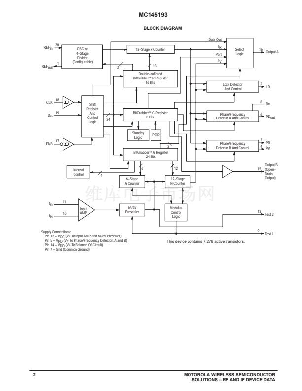
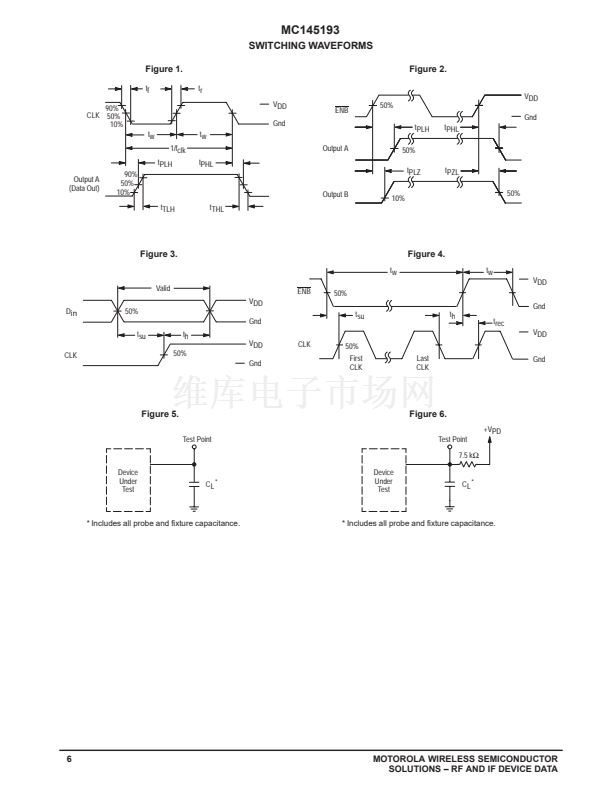
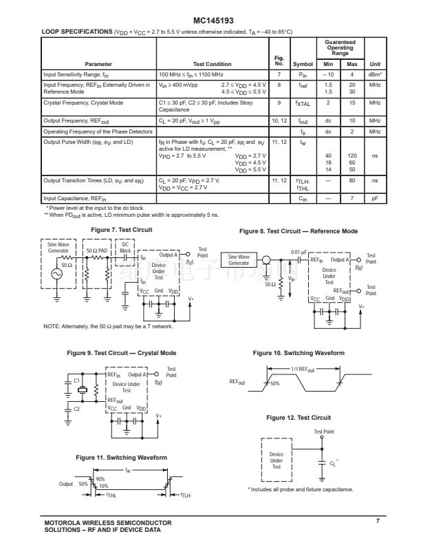
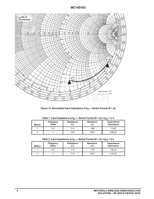
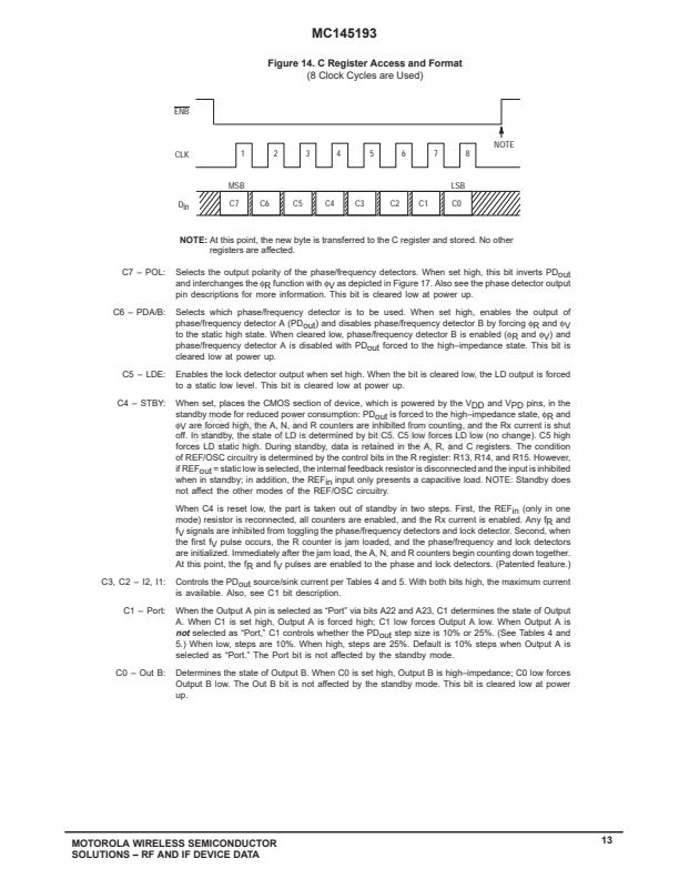
MC145193
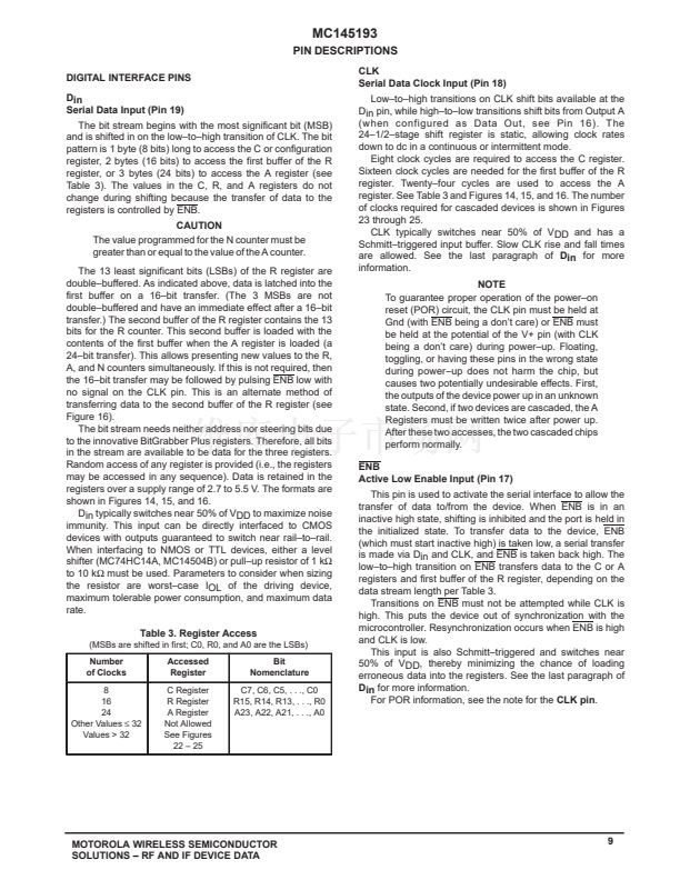
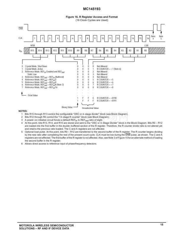
Figure 16. R Register Access and Format
(16 Clock Cycles are Used)
ENB
Note
4
Note
5
CLK
1
MSB
2
3
4
5
6
7
8
9
10
11
12
13
14
15
16
LSB
Din
R15
R14
R13
R12
R11
R10
R9
R8
R7
R6
R5
R4
R3
R2
R1
R0
0 Crystal Mode, Shut Down
1 Crystal Mode, Active
2 Reference Mode, REFin Enabled and REFout
Static Low
3 Reference Mode, REFout = REFin (Buffered)
4 Reference Mode, REFout = REFin/2
5 Reference Mode, REFout = REFin/4
6 Reference Mode, REFout = REFin/8 (Note 3)
7 Reference Mode, REFout = REFin/16
Octal Value
0
0
0
0
0
0
0
0
0
路
路
路
1
1
0
0
0
0
0
0
0
0
0
路
路
路
F
F
0
0
0
0
0
0
0
0
0
路
路
路
F
F
0
1
2
3
4
5
6
7
8
路
路
路
E
F
Not Allowed
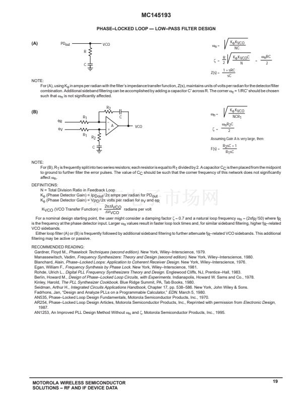
R COUNTER =
梅
1 (Note 6)
Not Allowed
Not Allowed
Not Allowed
R COUNTER =
梅
5
R COUNTER =
梅
6
R COUNTER =
梅
7
R COUNTER =
梅
8
R COUNTER =
梅
8190
R COUNTER =
梅
8191
Hexadecimal Value
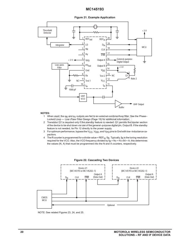
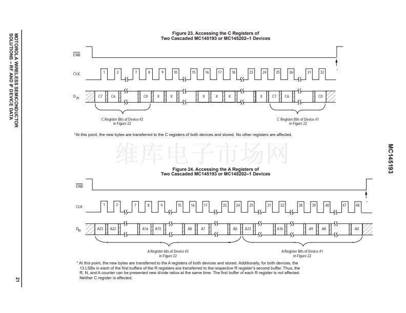
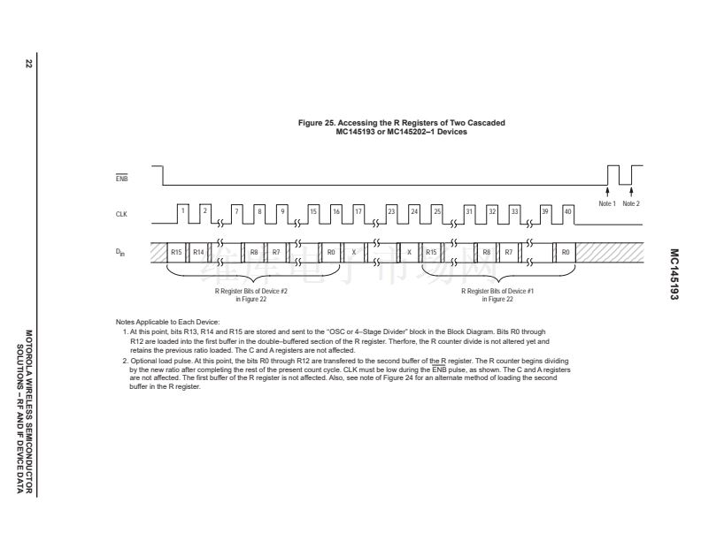
NOTES:
1 Bits R15 through R13 control the configurable 鈥淥SC or 4鈥搒tage divider鈥?block (see Block Diagram).
2 Bits R12 through R0 control the 鈥?3鈥搒tage R counter鈥?block (see Block Diagram).
3 A power鈥搊n initialize circuit forces a default REFin to REFout ratio of eight.
4 At this point, bits R13, R14, and R15 are stored and sent to the 鈥淥SC or 4鈥揝tage Divider鈥?block in the Block Diagram. Bits R0 鈥?R12
are loaded into the first buffer in the double鈥揵uffered section of the R register. Therefore, the R counter divide ratio is not altered yet
and retains the previous ratio loaded. The C and A registers are not affected.
5 Optional load pulse. At this point, bits R0 鈥?R12 are transferred to the second buffer of the R register. The R counter begins dividing
by the new ratio after completing the rest of the present count cycle. CLK must be low during the ENB pulse, as shown. The C and A
registers are not affected. The first buffer of the R register is not affected. Also, see Note 3 of Figure 15 for an alternate method of loading
the second buffer in the R register.
6 Allows direct access to reference input of phase/frequency detectors.
Binary Value
MOTOROLA WIRELESS SEMICONDUCTOR
SOLUTIONS 鈥?RF AND IF DEVICE DATA
15


 1
1
 2
2
 3
3
 4
4
 5
5
 6
6
 7
7
 8
8
 9
9
 10
10
 11
11
 12
12
 13
13
 14
14
 15
15
 16
16
 17
17
 18
18
 19
19
 20
20
 21
21
 22
22
 23
23
 24
24
