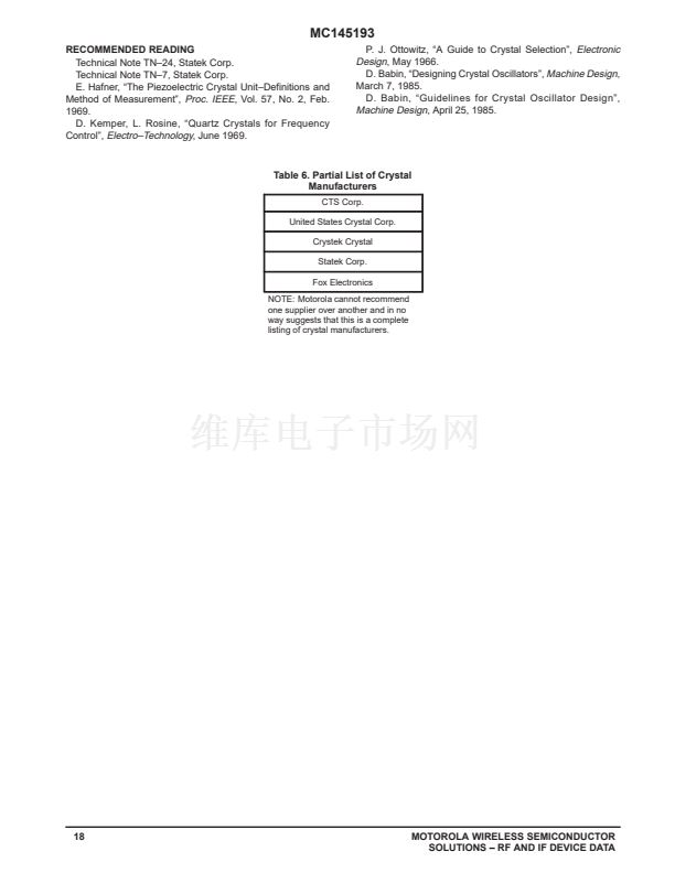
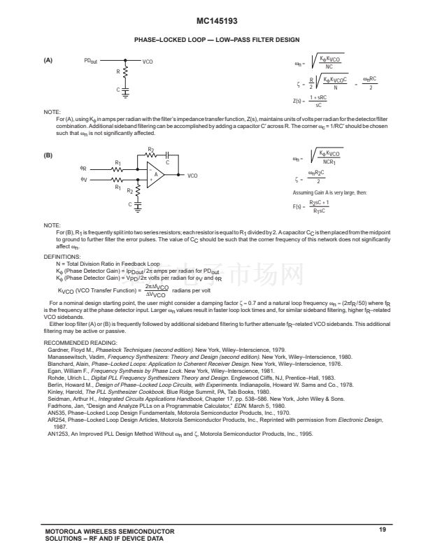
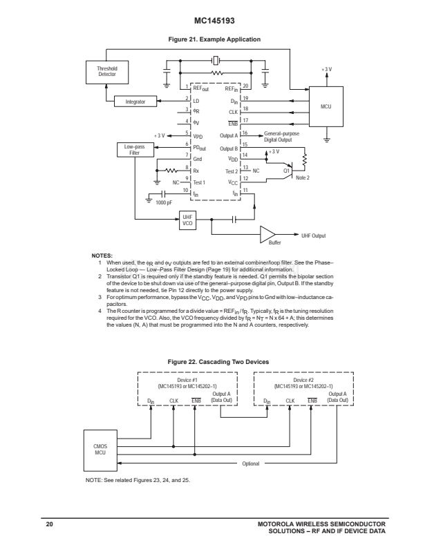
脟脟脟
脟脟脟
脟脟脟
脟脟脟
脟脟脟
脟脟脟
脟脟脟
脟脟脟
脟脟脟
脟脟脟
脟脟脟
脟脟脟
脟脟脟
脟脟脟
脟脟脟
脟脟脟
脟脟脟
脟脟脟
脟脟脟
脟脟脟
脟脟脟
脟脟脟
脟脟脟
脟脟脟
脟脟脟
脟脟脟
脟脟脟
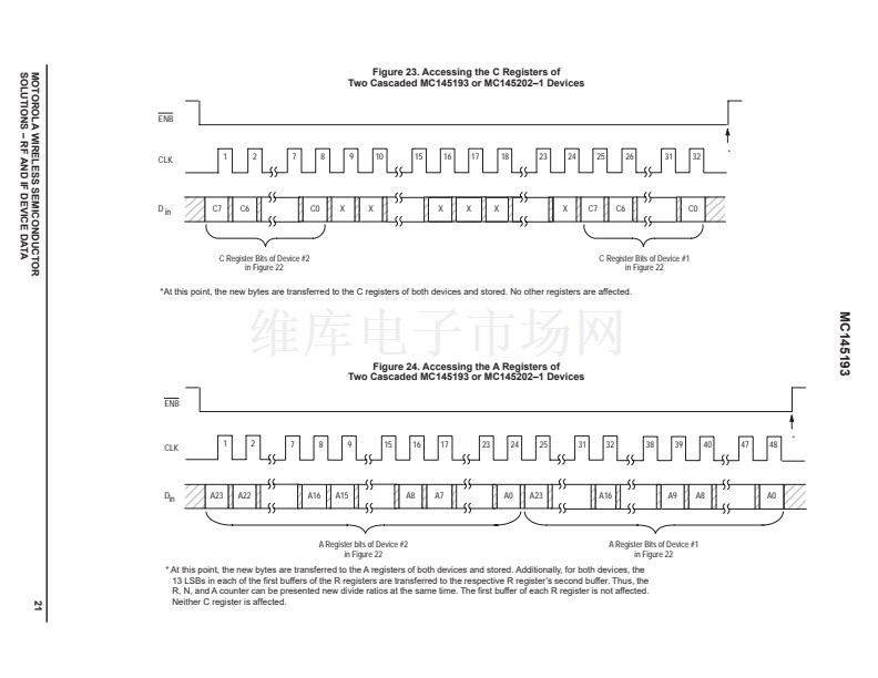
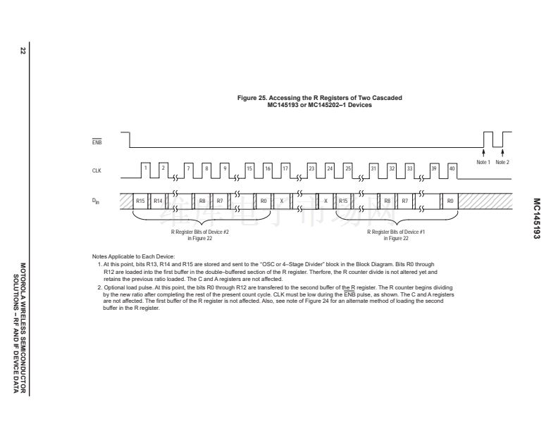
R8
R7
R0
X
X
R15
R8
R7
R0
R Register Bits of Device #2
in Figure 22
R Register Bits of Device #1
in Figure 22
22
Figure 25. Accessing the R Registers of Two Cascaded
MC145193 or MC145202鈥? Devices
ENB
Note 1 Note 2
CLK
1
2
7
8
9
15
16
17
23
24
25
31
32
33
39
40
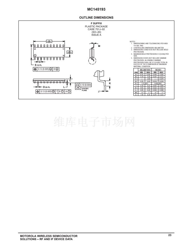
MC145193
Din
R15
R14
Figure 25.
Notes Applicable to Each Device:
1. At this point, bits R13, R14 and R15 are stored and sent to the 鈥樷€極SC or 4鈥揝tage Divider鈥?block in the Block Diagram. Bits R0 through
R12 are loaded into the first buffer in the double鈥揵uffered section of the R register. Therfore, the R counter divide is not altered yet and
retains the previous ratio loaded. The C and A registers are not affected.
2. Optional load pulse. At this point, the bits R0 through R12 are transfered to the second buffer of the R register. The R counter begins dividing
by the new ratio after completing the rest of the present count cycle. CLK must be low during the ENB pulse, as shown. The C and A registers
are not affected. The first buffer of the R register is not affected. Also, see note of Figure 24 for an alternate method of loading the second
buffer in the R register.
MOTOROLA WIRELESS SEMICONDUCTOR
SOLUTIONS 鈥?RF AND IF DEVICE DATA


 1
1
 2
2
 3
3
 4
4
 5
5
 6
6
 7
7
 8
8
 9
9
 10
10
 11
11
 12
12
 13
13
 14
14
 15
15
 16
16
 17
17
 18
18
 19
19
 20
20
 21
21
 22
22
 23
23
 24
24
