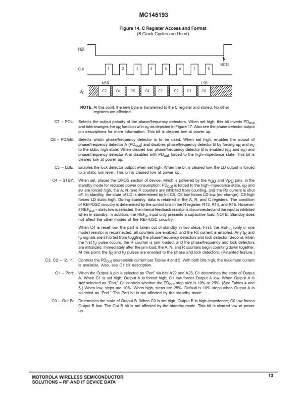
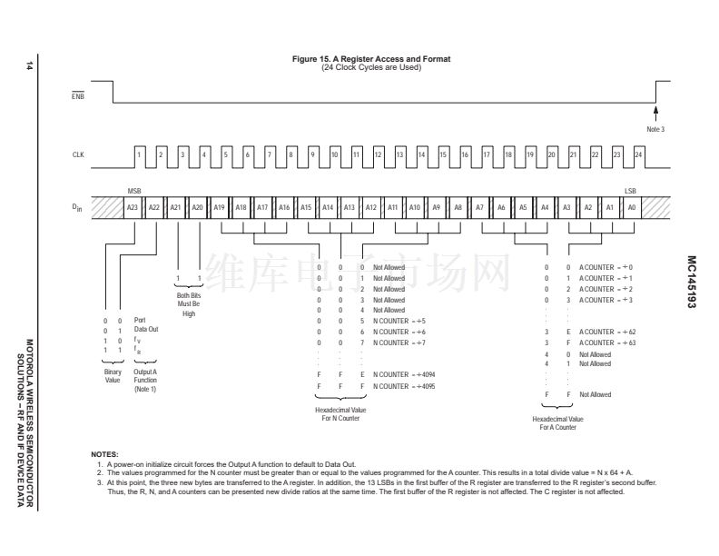
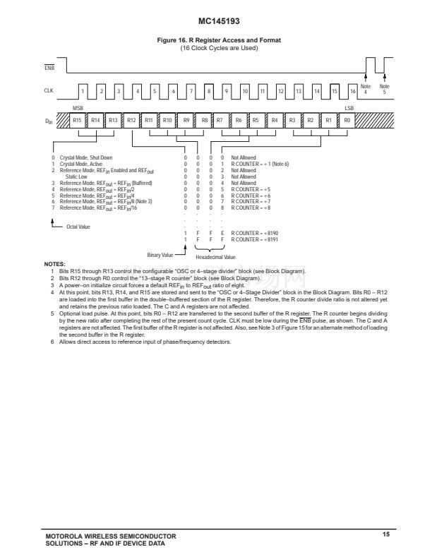
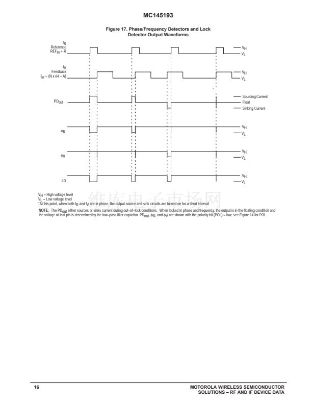
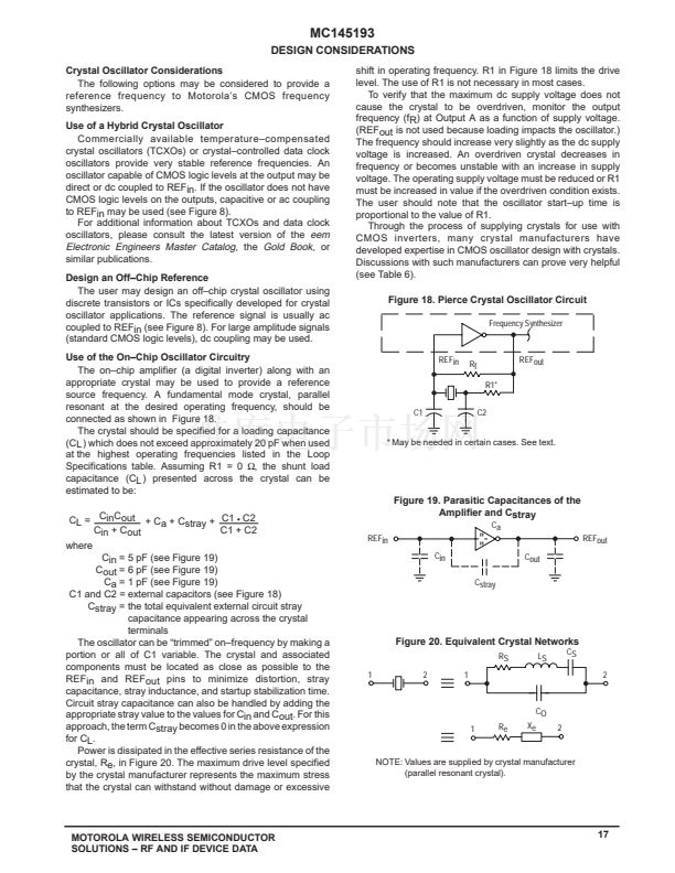
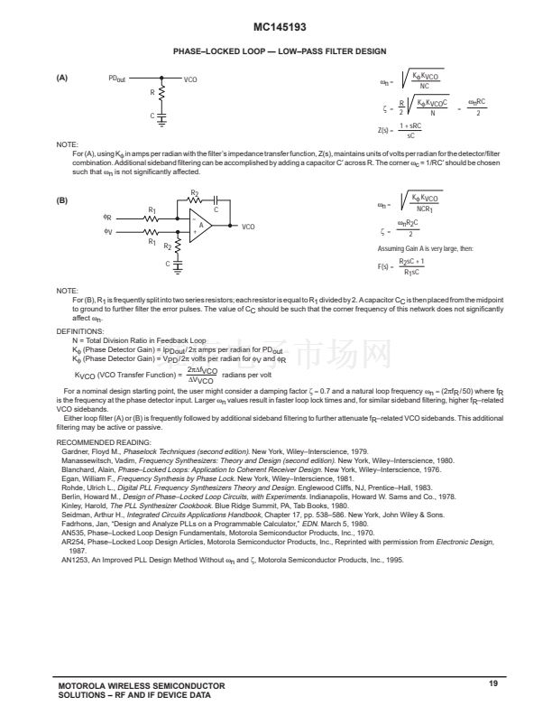
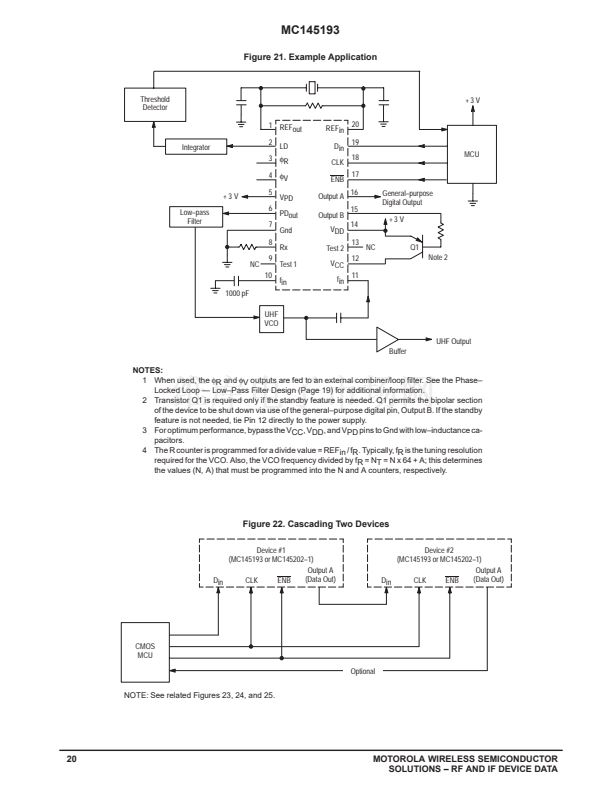
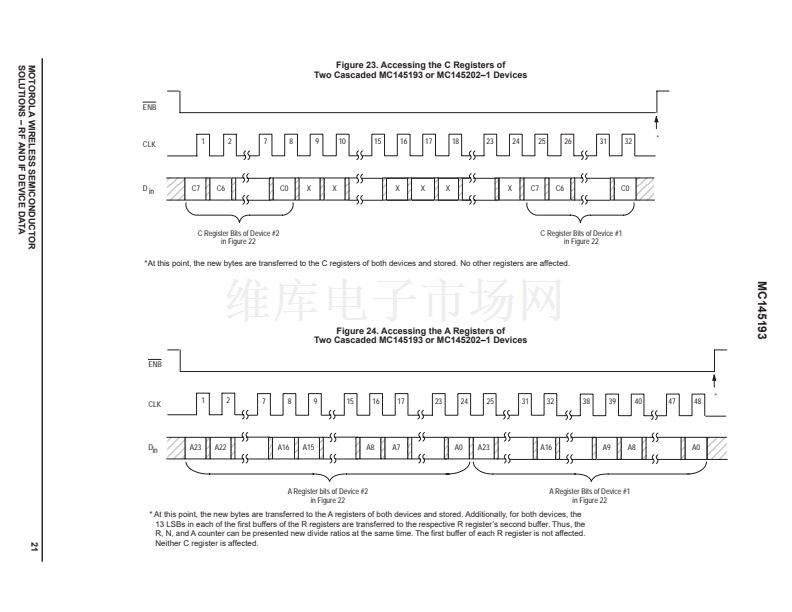
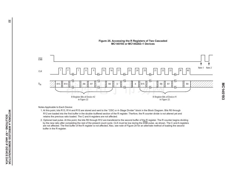
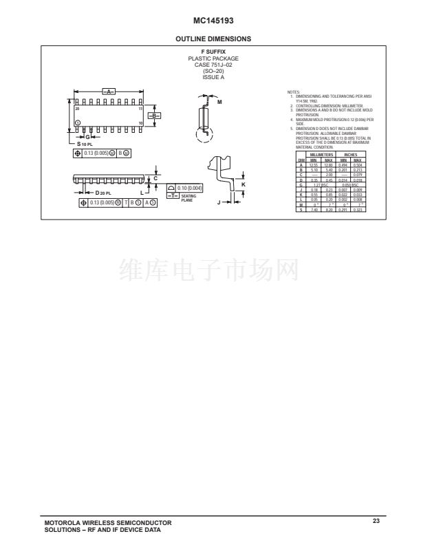
MC145193
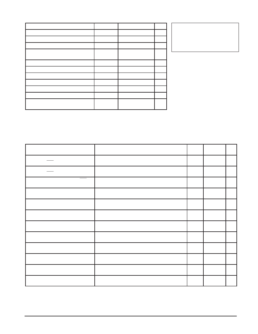
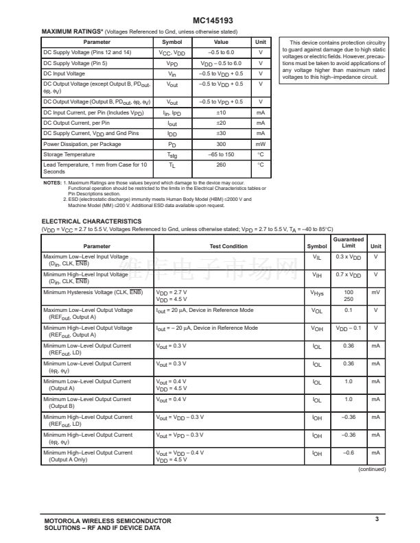
MAXIMUM RATINGS*
(Voltages Referenced to Gnd, unless otherwise stated)
Parameter
DC Supply Voltage (Pins 12 and 14)
DC Supply Voltage (Pin 5)
DC Input Voltage
DC Output Voltage (except Output B, PDout,
蠁
R,
蠁
V)
DC Output Voltage (Output B, PDout,
蠁
R,
蠁
V)
DC Input Current, per Pin (Includes VPD)
DC Output Current, per Pin
DC Supply Current, VDD and Gnd Pins
Power Dissipation, per Package
Storage Temperature
Lead Temperature, 1 mm from Case for 10
Seconds
Symbol
VCC, VDD
VPD
Vin
Vout
Vout
Iin, IPD
Iout
IDD
PD
Tstg
TL
Value
鈥?.5 to 6.0
VDD 鈥?0.5 to 6.0
鈥?.5 to VDD + 0.5
鈥?.5 to VDD + 0.5
鈥?.5 to VPD + 0.5
卤10
卤20
卤30
300
鈥?5 to 150
260
Unit
V
V
V
V
V
mA
mA
mA
mW
掳C
掳C
This device contains protection circuitry
to guard against damage due to high static
voltages or electric fields. However, precau-
tions must be taken to avoid applications of
any voltage higher than maximum rated
voltages to this high鈥搃mpedance circuit.
NOTES:
1. Maximum Ratings are those values beyond which damage to the device may occur.
Functional operation should be restricted to the limits in the Electrical Characteristics tables or
Pin Descriptions section.
2. ESD (electrostatic discharge) immunity meets Human Body Model (HBM)
鈮?000
V and
Machine Model (MM)
鈮?00
V. Additional ESD data available upon request.
ELECTRICAL CHARACTERISTICS
(VDD = VCC = 2.7 to 5.5 V, Voltages Referenced to Gnd, unless otherwise stated; VPD = 2.7 to 5.5 V, TA = 鈥?0 to 85掳C)
Parameter
Maximum Low鈥揕evel Input Voltage
(Din, CLK, ENB)
Minimum High鈥揕evel Input Voltage
(Din, CLK, ENB)
Minimum Hysteresis Voltage (CLK, ENB)
Maximum Low鈥揕evel Output Voltage
(REFout, Output A)
Minimum High鈥揕evel Output Voltage
(REFout, Output A)
Minimum Low鈥揕evel Output Current
(REFout, LD)
Minimum Low鈥揕evel Output Current
(蠁R,
蠁
V)
Minimum Low鈥揕evel Output Current
(Output A)
Minimum Low鈥揕evel Output Current
(Output B)
Minimum High鈥揕evel Output Current
(REFout, LD)
Minimum High鈥揕evel Output Current
(蠁R,
蠁
V)
Minimum High鈥揕evel Output Current
(Output A Only)
VDD = 2.7 V
VDD = 4.5 V
Iout = 20
碌A,
Device in Reference Mode
Iout = 鈥?20
碌A,
Device in Reference Mode
Vout = 0.3 V
Vout = 0.3 V
Vout = 0.4 V
VDD = 4.5 V
Vout = 0.4 V
Vout = VDD 鈥?0.3 V
Vout = VPD 鈥?0.3 V
Vout = VDD 鈥?0.4 V
VDD = 4.5 V
Test Condition
Symbol
VIL
VIH
VHys
VOL
VOH
IOL
IOL
IOL
IOL
IOH
IOH
IOH
Guaranteed
Limit
0.3 x VDD
0.7 x VDD
100
250
0.1
VDD 鈥?0.1
0.36
0.36
1.0
1.0
鈥?.36
鈥?.36
鈥?.6
Unit
V
V
mV
V
V
mA
mA
mA
mA
mA
mA
mA
(continued)
MOTOROLA WIRELESS SEMICONDUCTOR
SOLUTIONS 鈥?RF AND IF DEVICE DATA
3


 1
1
 2
2
 3
3
 4
4
 5
5
 6
6
 7
7
 8
8
 9
9
 10
10
 11
11
 12
12
 13
13
 14
14
 15
15
 16
16
 17
17
 18
18
 19
19
 20
20
 21
21
 22
22
 23
23
 24
24
