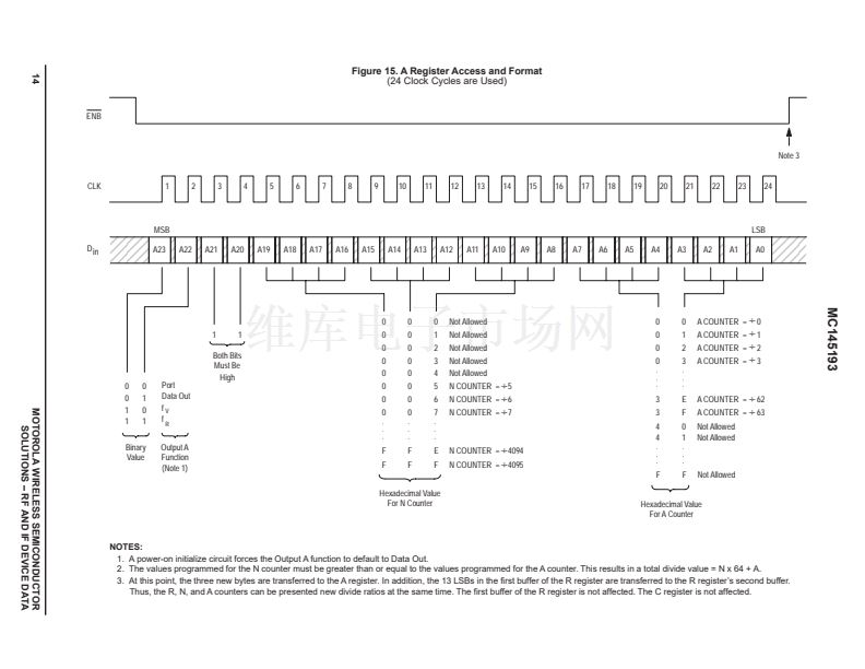
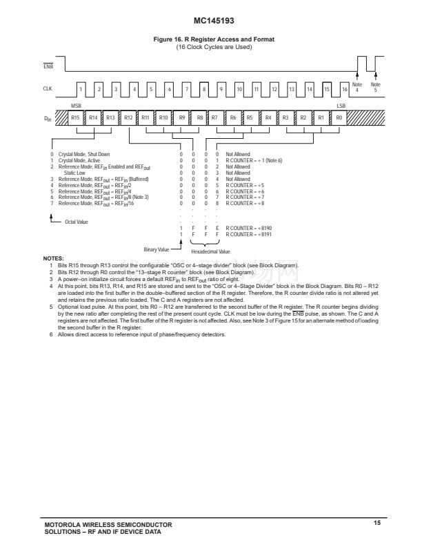
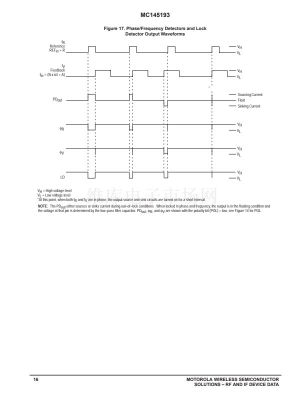
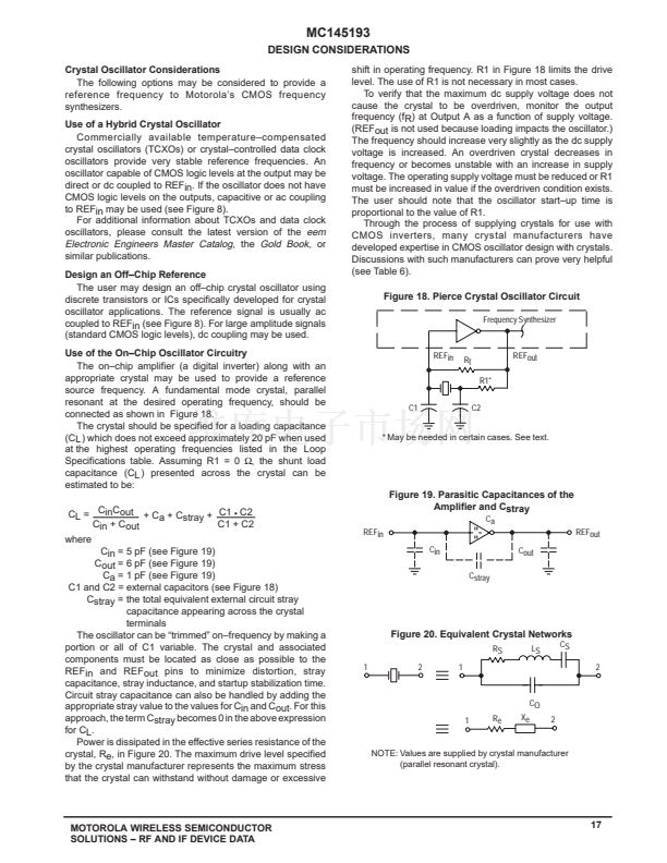
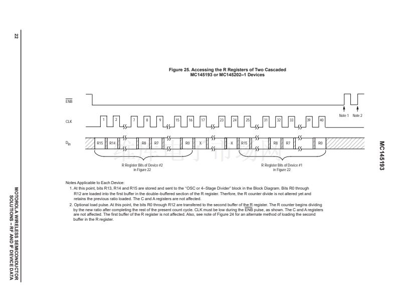
MC145193
AC INTERFACE CHARACTERISTICS
(VDD = VCC = 2.7 to 5.5 V, TA = 鈥?40 to + 85掳C, CL = 25 pF, Input tr = tf = 10 ns; VPD = 2.7 to 5.5 V)
Parameter
Serial Data Clock Frequency (Note: Refer to Clock tw below)
Maximum Propagation Delay, CLK to Output A (Selected as Data Out)
Maximum Propagation Delay, ENB to Output A (Selected as Port)
Maximum Propagation Delay, ENB to Output B
Maximum Output Transition Time, Output A and Output B; tTHLonly, on Output B
Maximum Input Capacitance 鈥?Din, ENB, CLK
Figure
No.
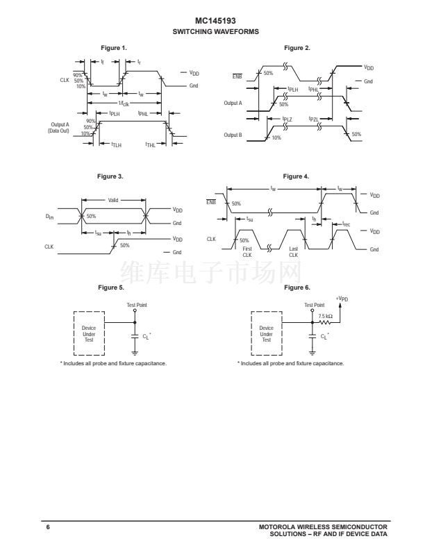
1
1, 5
2, 5
2, 6
1, 5, 6
Symbol
fclk
tPLH, tPHL
tPLH, tPHL
tPZL, tPLZ
tTLH, tTHL
Cin
Guaranteed
Limit
dc to 4.0
100
150
150
50
10
Unit
MHz
ns
ns
ns
ns
pF
TIMING REQUIREMENTS
(VDD = VCC = 2.7 to 5.5 V, TA = 鈥?40 to + 85掳C, Input tr = tf = 10 ns, unless otherwise indicated)
Parameter
Minimum Setup and Hold Times, Din vs CLK
Minimum Setup, Hold and Recovery Times, ENB vs CLK
Minimum Pulse Width, ENB
Minimum Pulse Width, CLK
Maximum Input Rise and Fall Times, CLK
NOTE:
The minimum limit is 3 REFin cycles or 195 fin cycles, whichever is greater.
Figure
No.
3
4
4
1
1
Symbol
tsu, th
tsu, th, trec
tw
tw
tr, tf
Guaranteed
Limit
50
100
[Note]
125
100
Unit
ns
ns
cycles
ns
碌s
MOTOROLA WIRELESS SEMICONDUCTOR
SOLUTIONS 鈥?RF AND IF DEVICE DATA
5


 1
1
 2
2
 3
3
 4
4
 5
5
 6
6
 7
7
 8
8
 9
9
 10
10
 11
11
 12
12
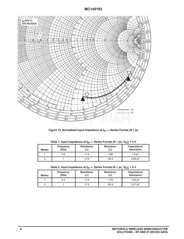
 13
13
 14
14
 15
15
 16
16
 17
17
 18
18
 19
19
 20
20
 21
21
 22
22
 23
23
 24
24
