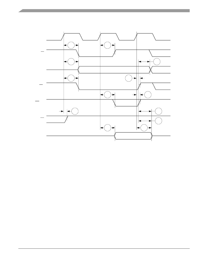
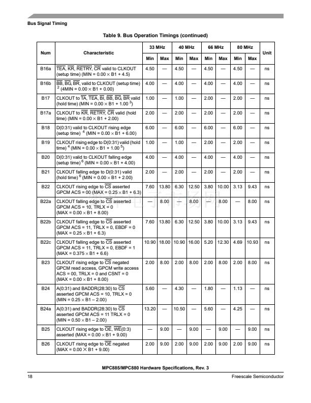
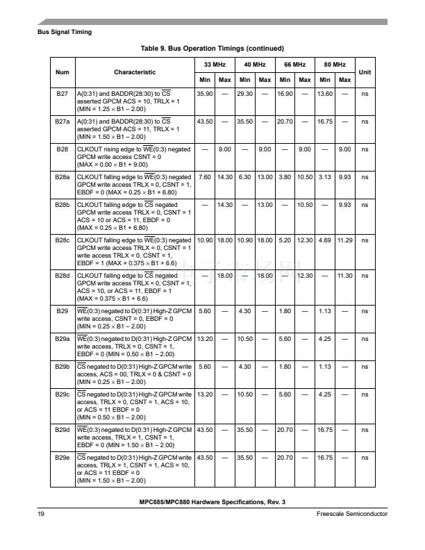
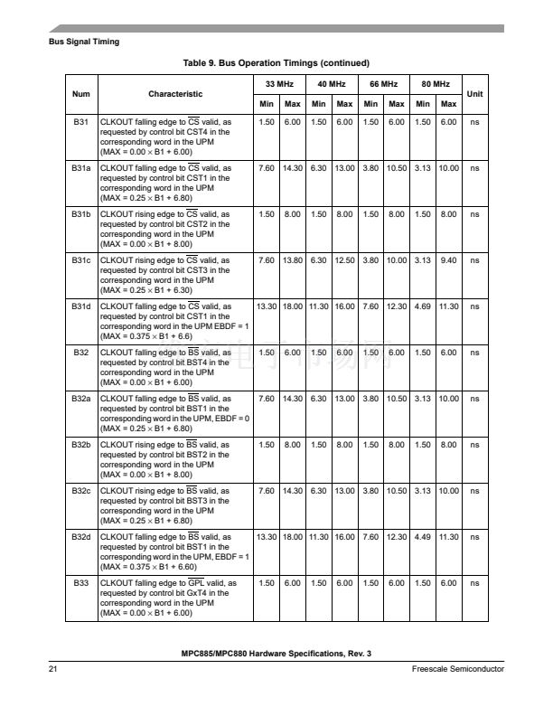
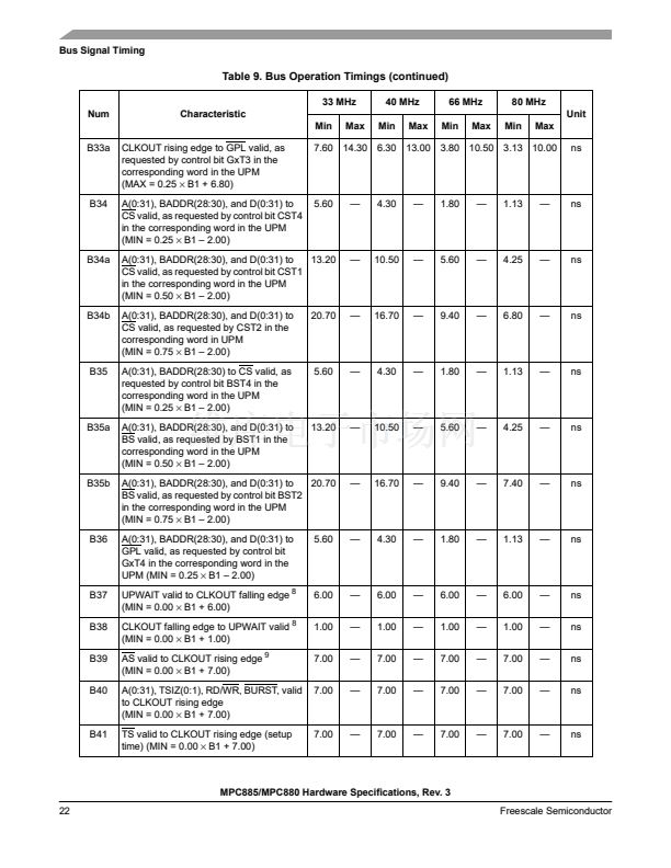
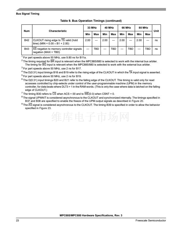
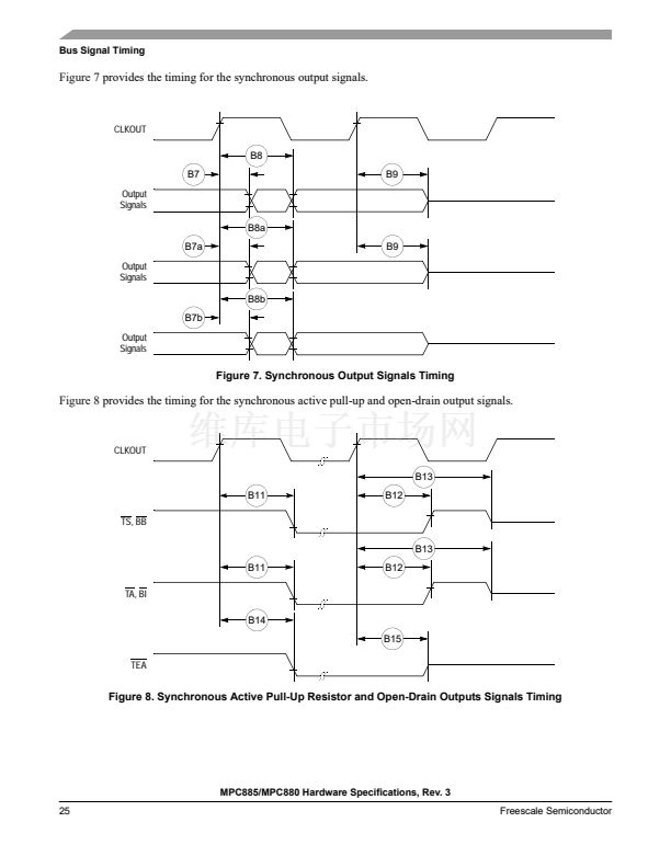
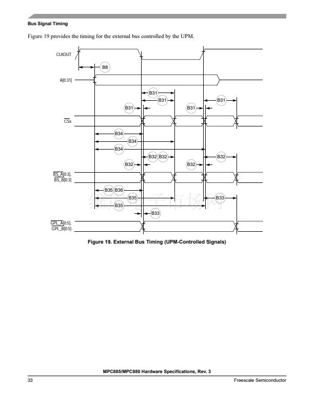
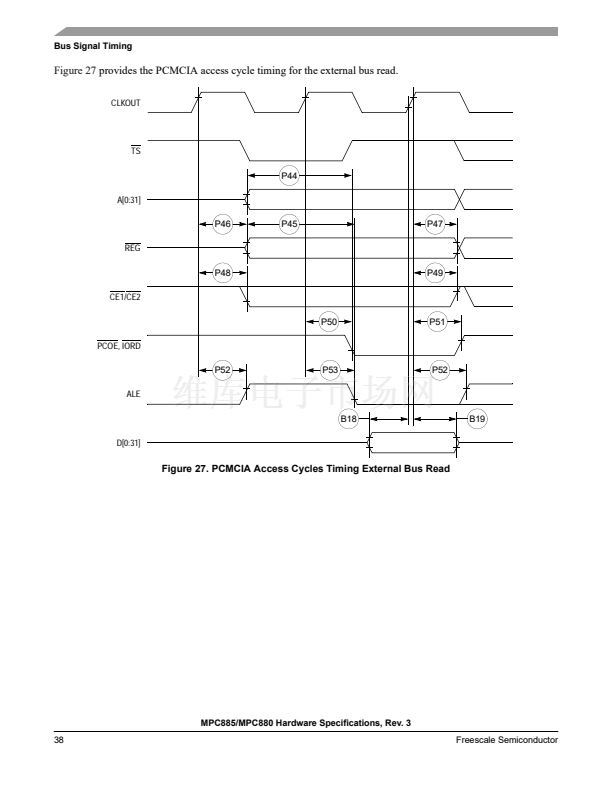
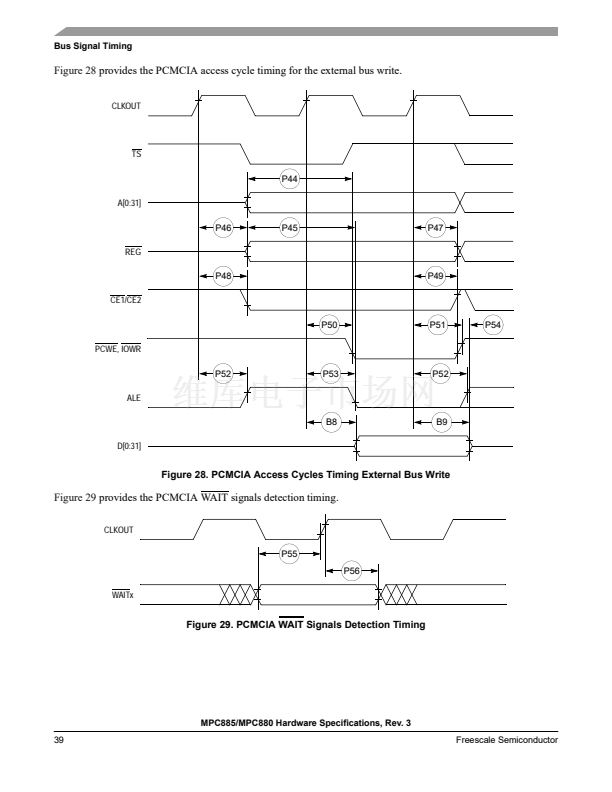
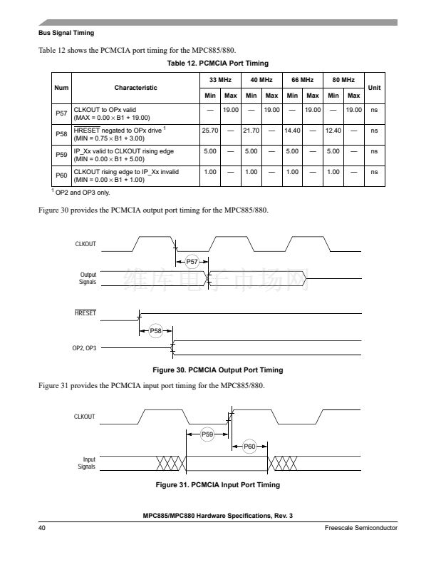
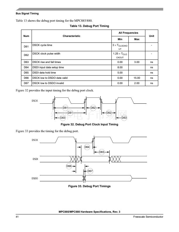
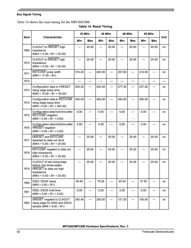
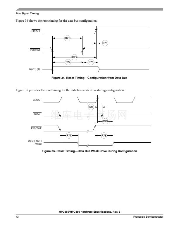
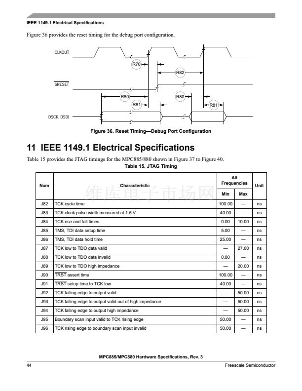
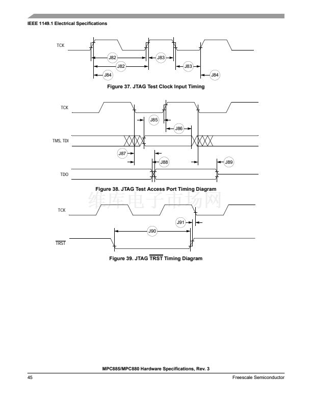
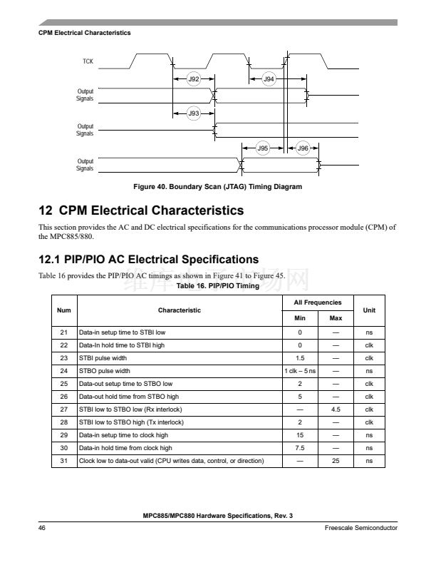
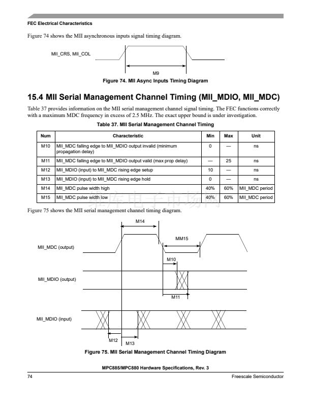
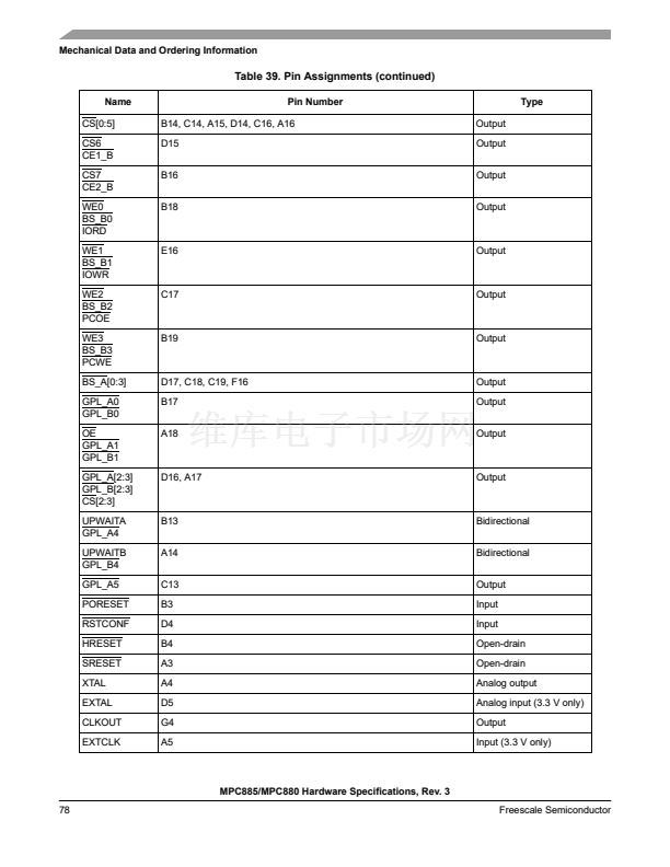
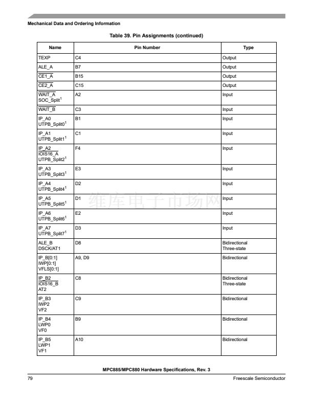
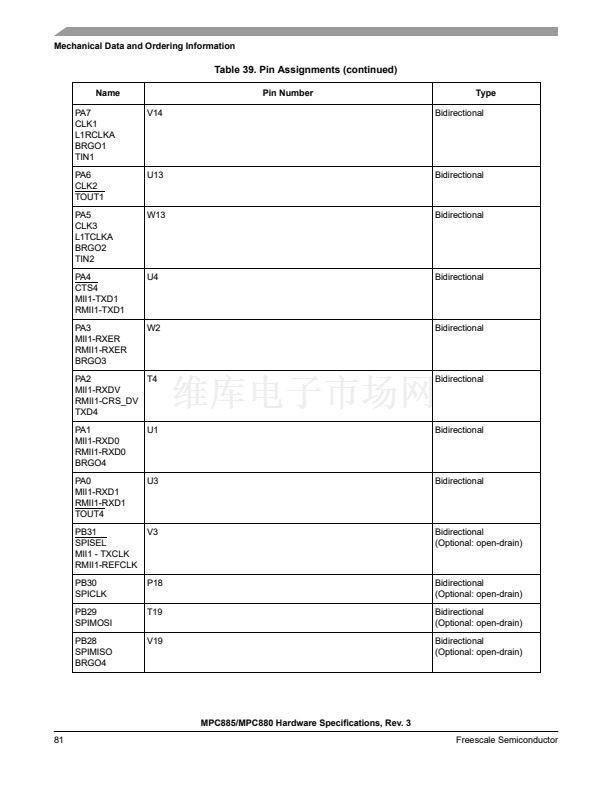
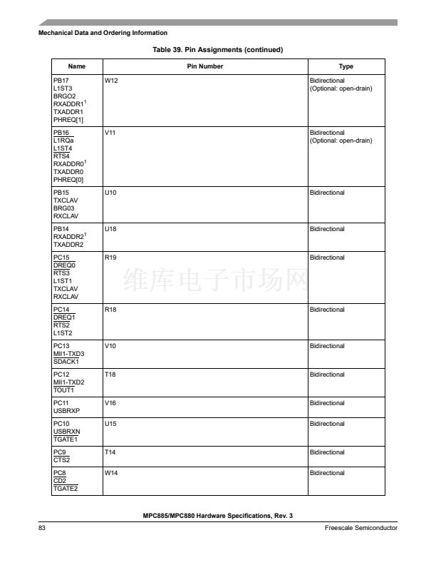
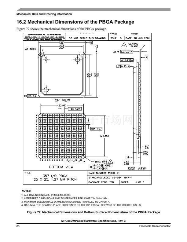
Bus Signal Timing
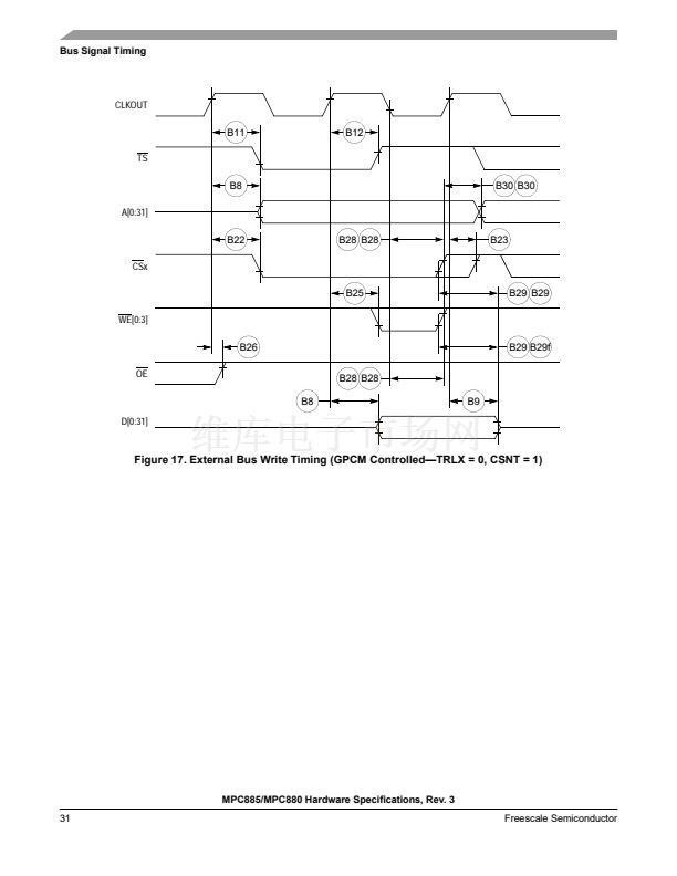
Figure 16
through
Figure 18
provide the timing for the external bus write controlled by various GPCM factors.
CLKOUT
B11
TS
B8
A[0:31]
B22
CSx
B25
WE[0:3]
B26
OE
B8
D[0:31]
B9
B29
B29
B28
B23
B30
B12
Figure 16. External Bus Write Timing (GPCM Controlled鈥擳RLX = 0, CSNT = 0)
MPC885/MPC880 Hardware Specifications, Rev. 3
30
Freescale Semiconductor


 1
1
 2
2
 3
3
 4
4
 5
5
 6
6
 7
7
 8
8
 9
9
 10
10
 11
11
 12
12
 13
13
 14
14
 15
15
 16
16
 17
17
 18
18
 19
19
 20
20
 21
21
 22
22
 23
23
 24
24
 25
25
 26
26
 27
27
 28
28
 29
29
 30
30
 31
31
 32
32
 33
33
 34
34
 35
35
 36
36
 37
37
 38
38
 39
39
 40
40
 41
41
 42
42
 43
43
 44
44
 45
45
 46
46
 47
47
 48
48
 49
49
 50
50
 51
51
 52
52
 53
53
 54
54
 55
55
 56
56
 57
57
 58
58
 59
59
 60
60
 61
61
 62
62
 63
63
 64
64
 65
65
 66
66
 67
67
 68
68
 69
69
 70
70
 71
71
 72
72
 73
73
 74
74
 75
75
 76
76
 77
77
 78
78
 79
79
 80
80
 81
81
 82
82
 83
83
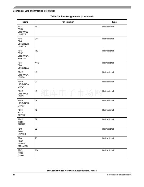 84
84
 85
85
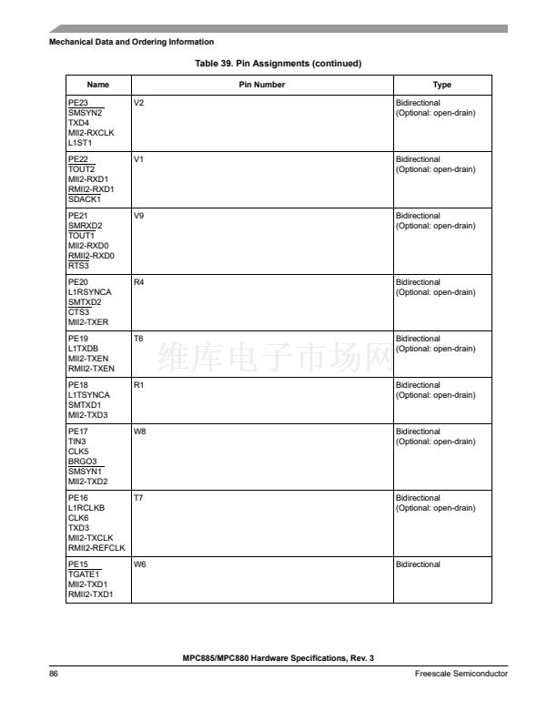 86
86
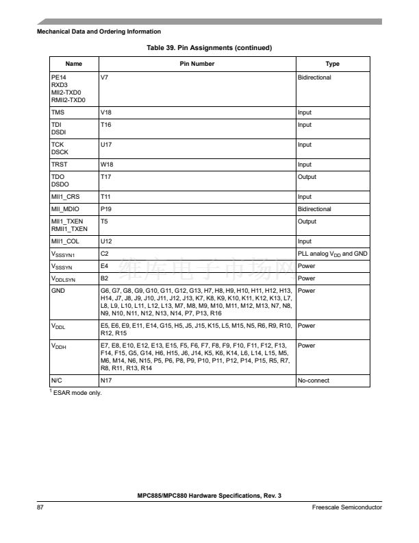 87
87
 88
88
 89
89
 90
90
 91
91
 92
92
