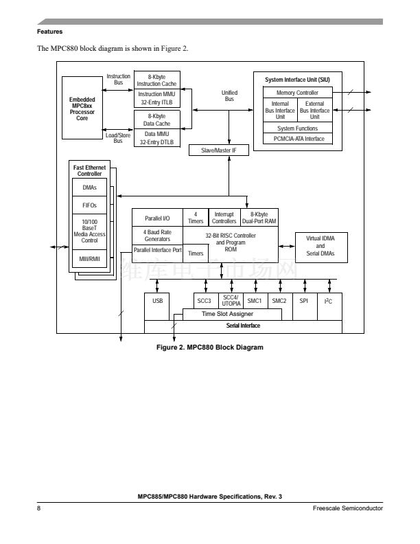
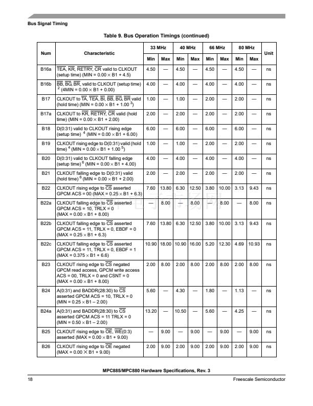
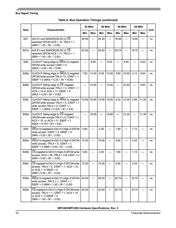
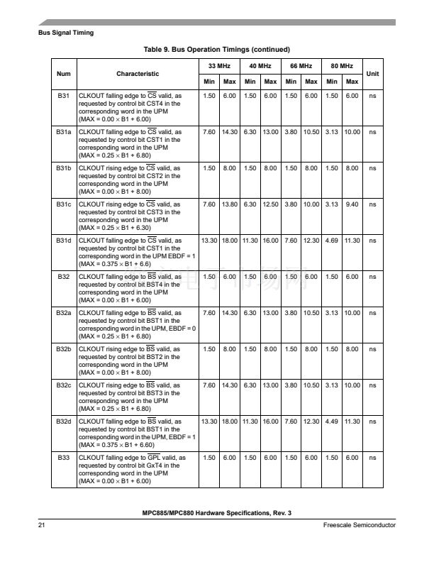
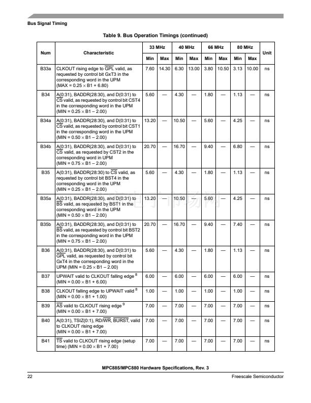
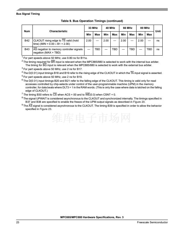
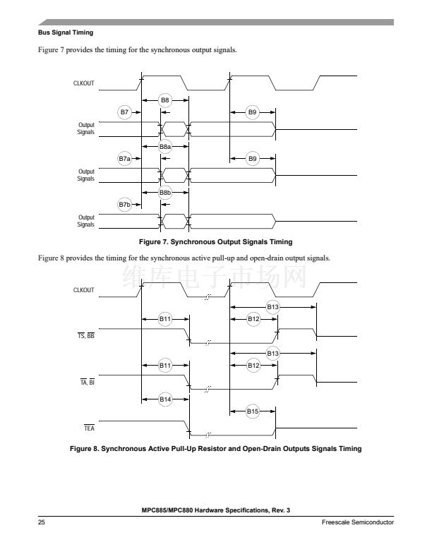
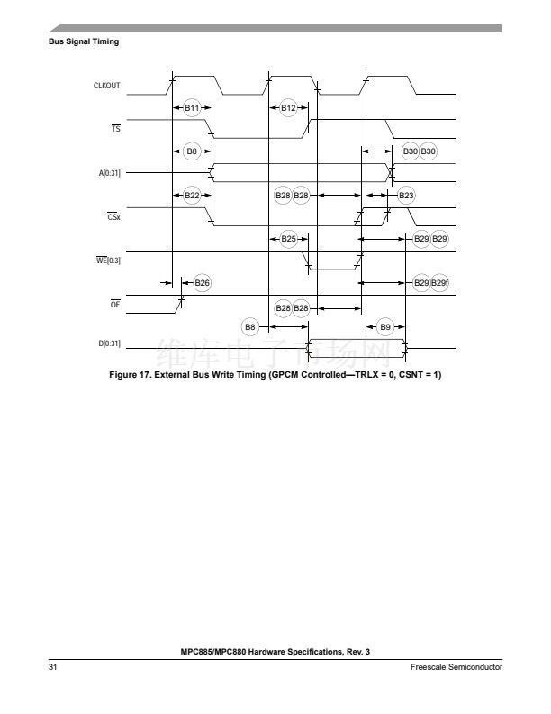
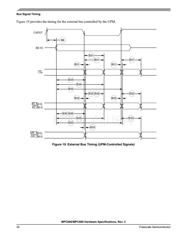
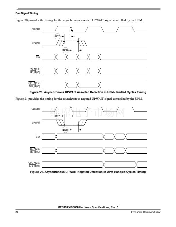
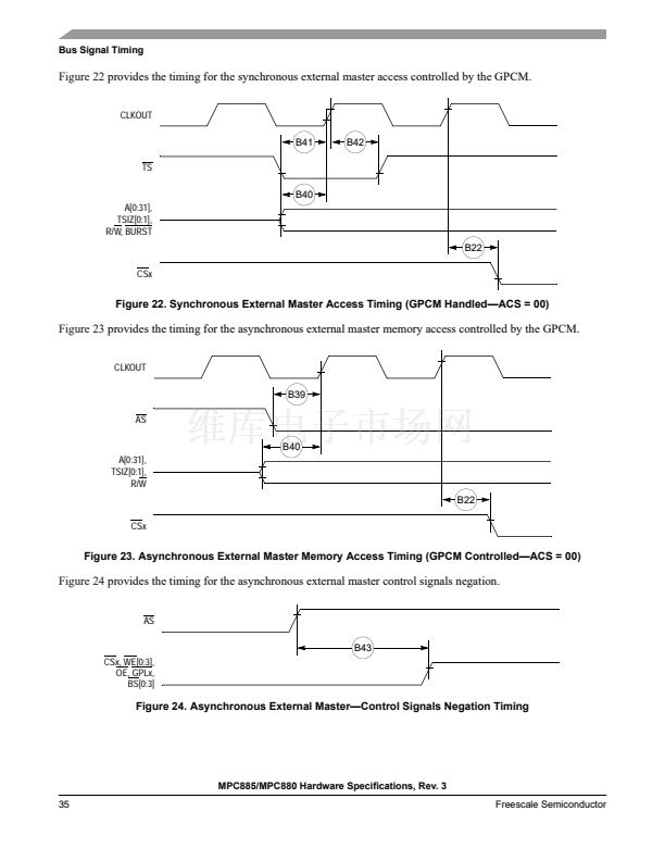
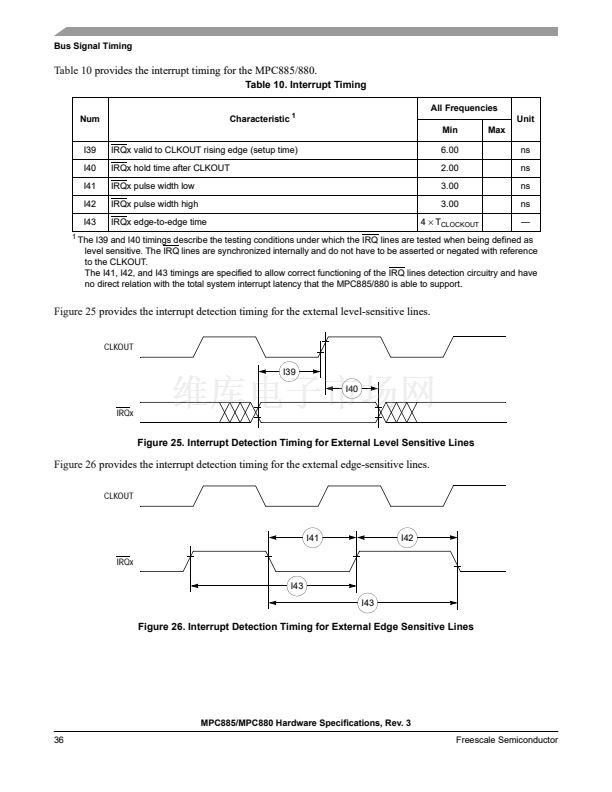
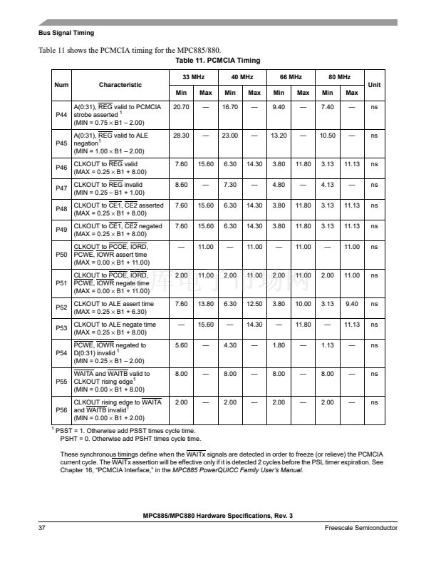
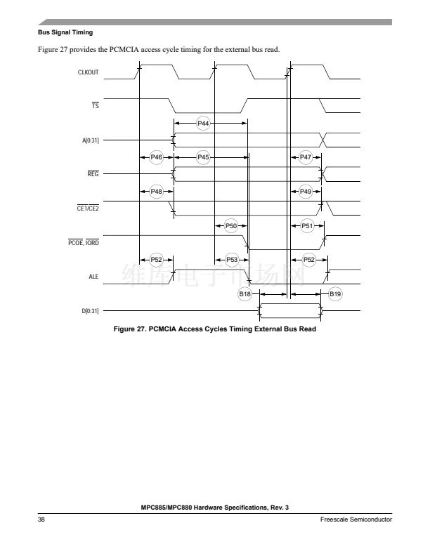
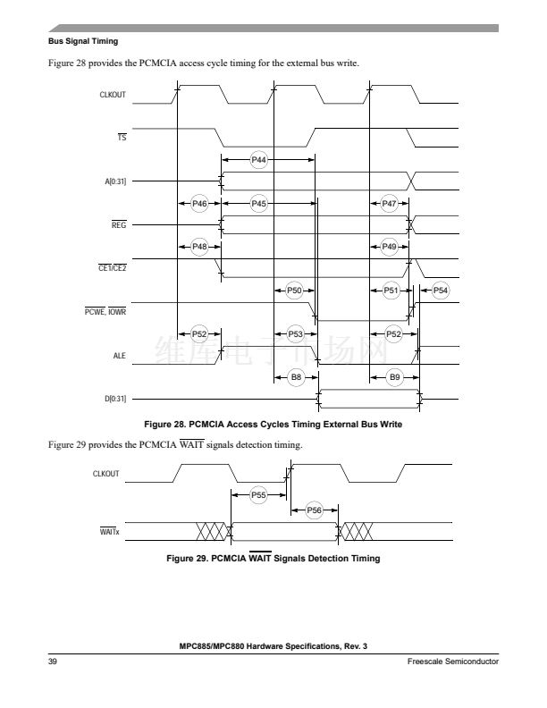
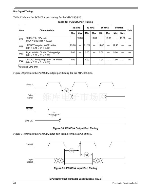
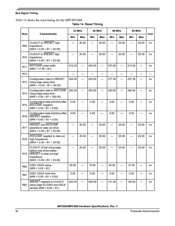
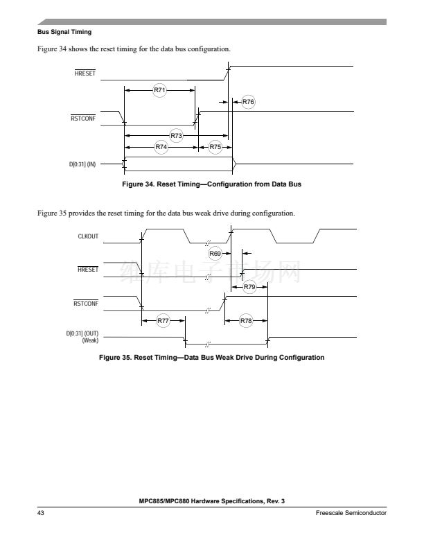
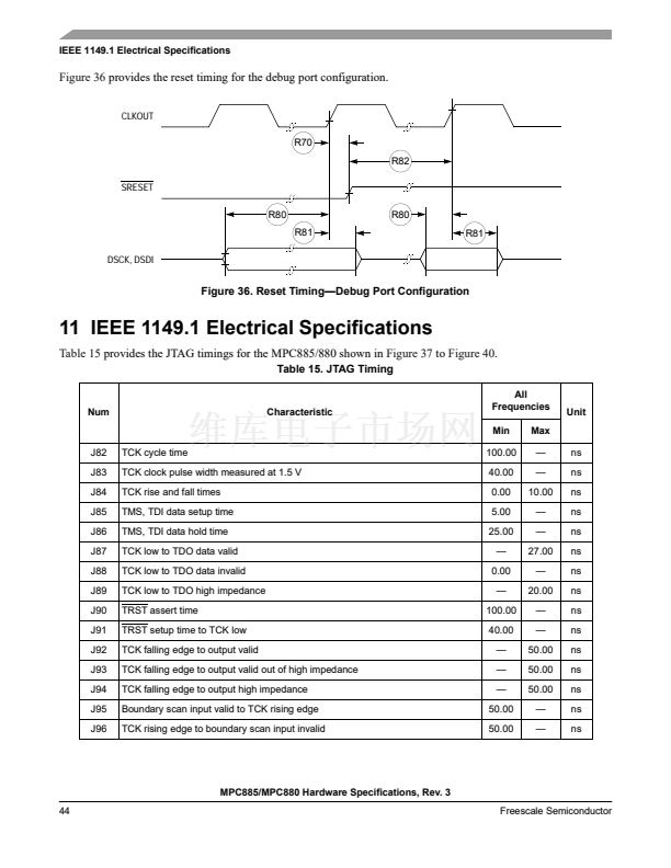
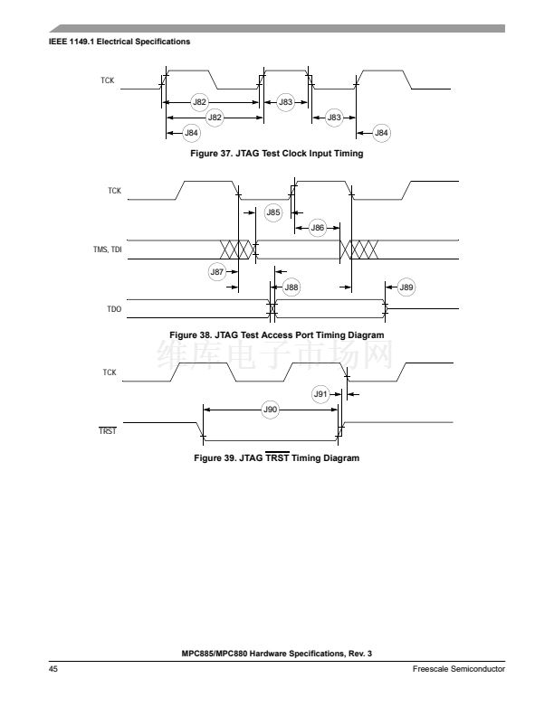
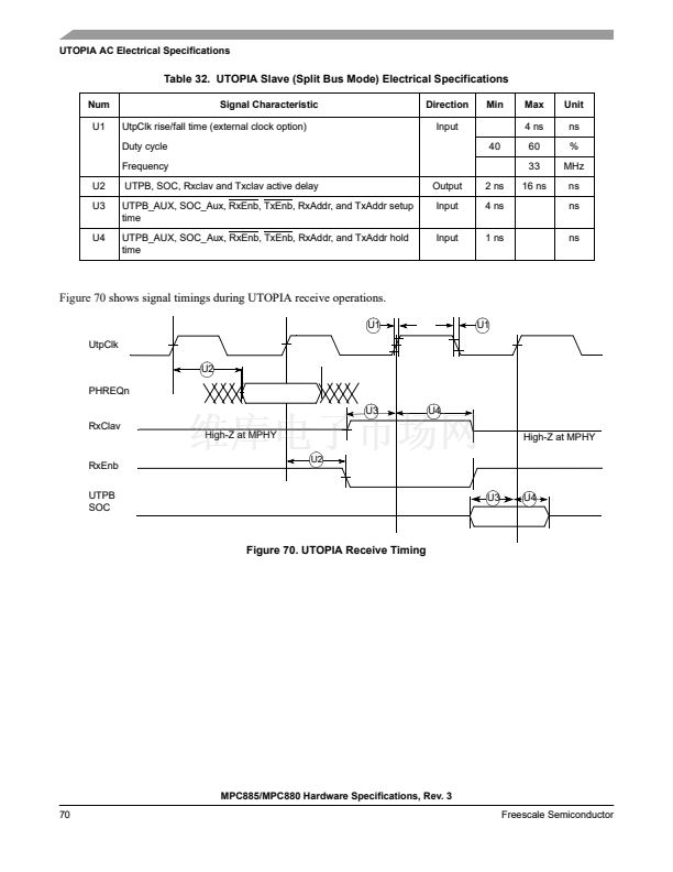
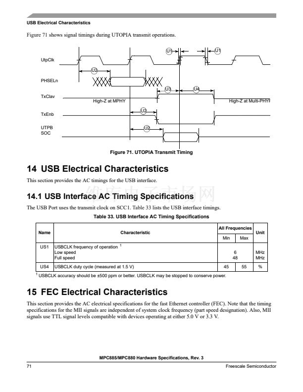
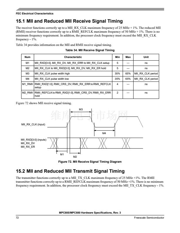
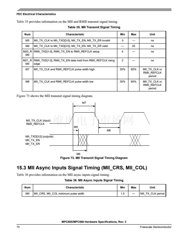
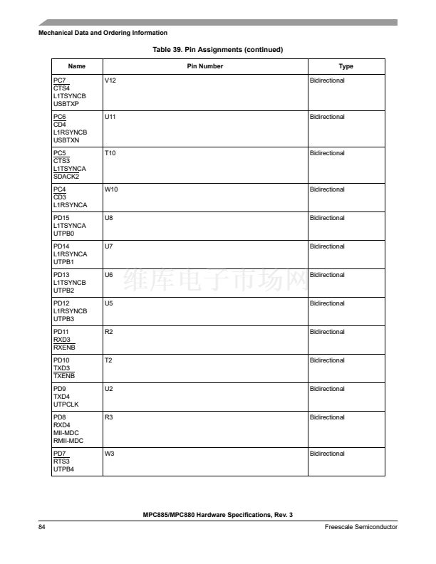
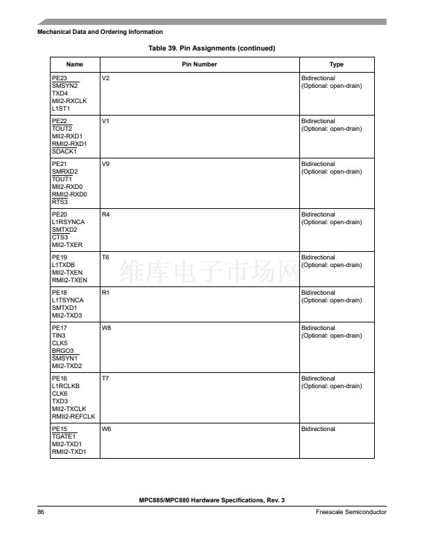
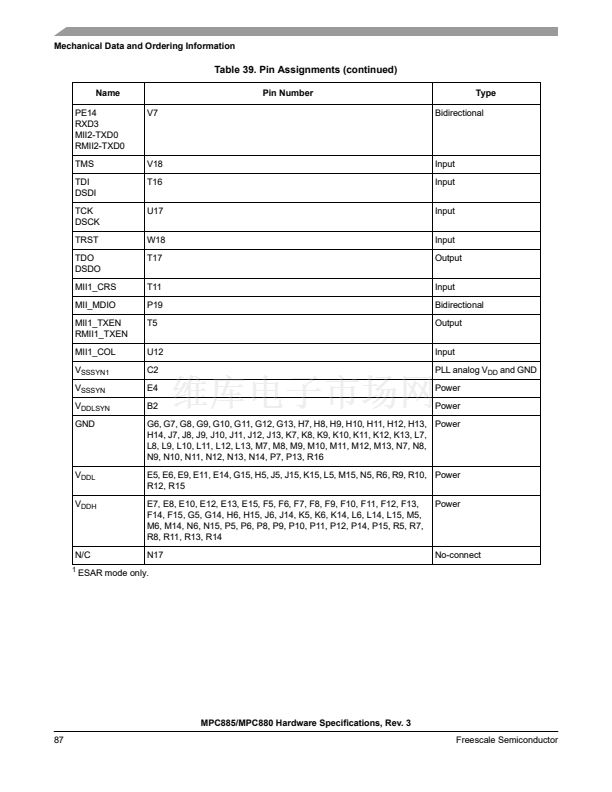
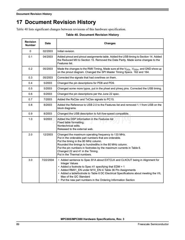
Bus Signal Timing
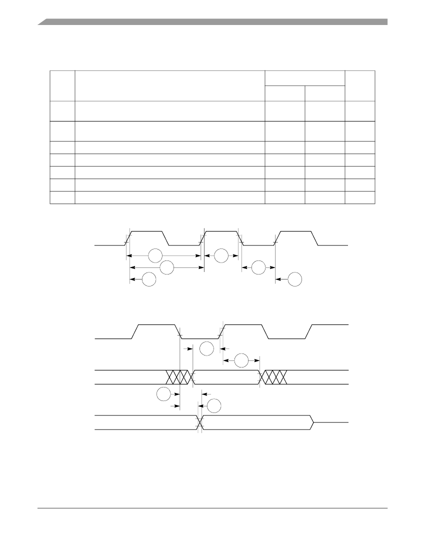
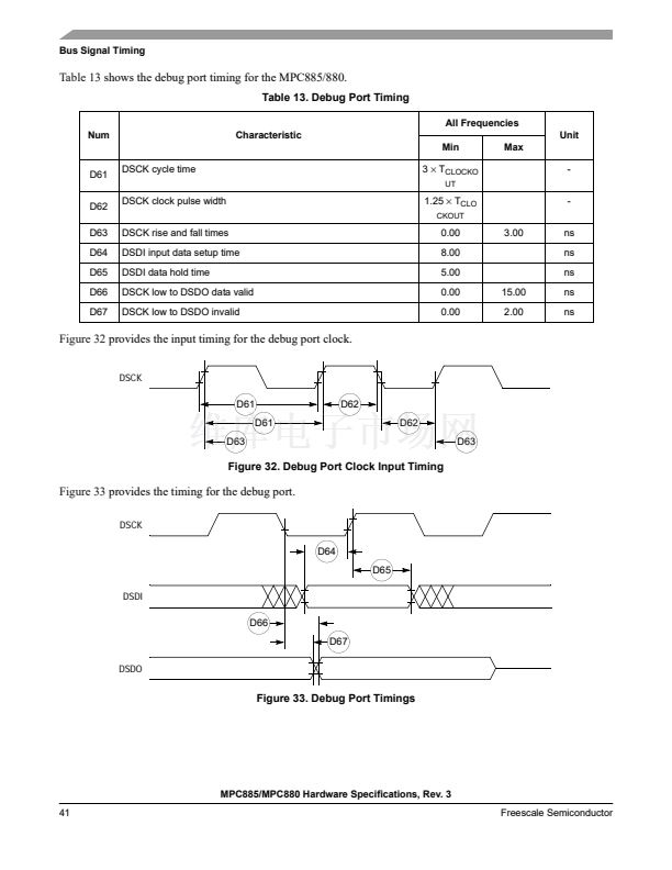
Table 13
shows the debug port timing for the MPC885/880.
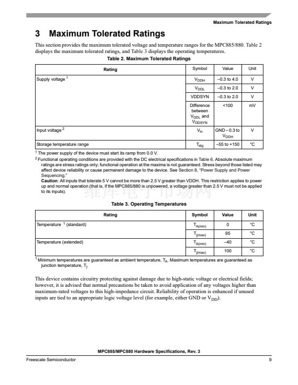
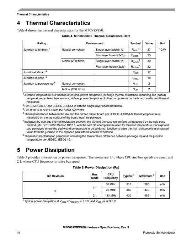
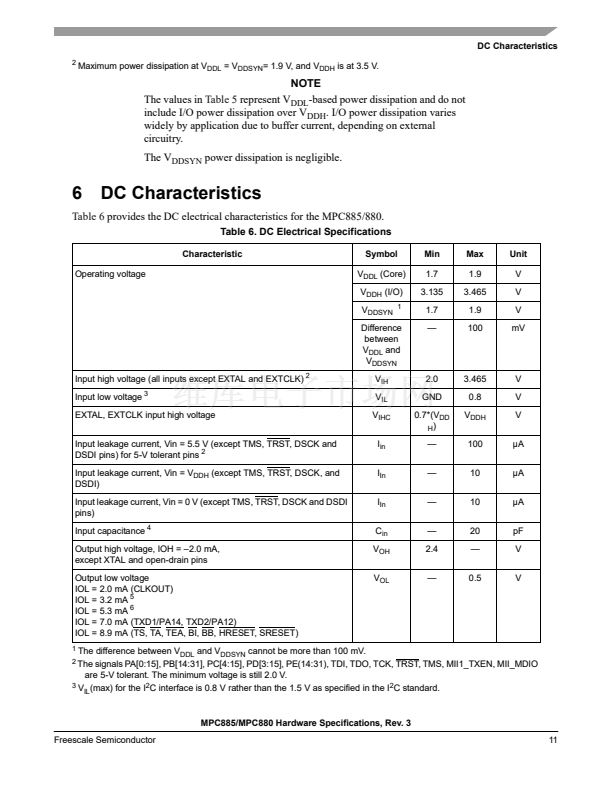
Table 13. Debug Port Timing
All Frequencies
Num
Characteristic
Min
D61
D62
D63
D64
D65
D66
D67
DSCK cycle time
DSCK clock pulse width
DSCK rise and fall times
DSDI input data setup time
DSDI data hold time
DSCK low to DSDO data valid
DSCK low to DSDO invalid
3
脳
T
CLOCKO
UT
Unit
Max
-
-
3.00
ns
ns
ns
15.00
2.00
ns
ns
1.25
脳
T
CLO
CKOUT
0.00
8.00
5.00
0.00
0.00
Figure 32
provides the input timing for the debug port clock.
DSCK
D61
D61
D63
D62
D62
D63
Figure 32. Debug Port Clock Input Timing
Figure 33
provides the timing for the debug port.
DSCK
D64
D65
DSDI
D66
D67
DSDO
Figure 33. Debug Port Timings
MPC885/MPC880 Hardware Specifications, Rev. 3
41
Freescale Semiconductor


 1
1
 2
2
 3
3
 4
4
 5
5
 6
6
 7
7
 8
8
 9
9
 10
10
 11
11
 12
12
 13
13
 14
14
 15
15
 16
16
 17
17
 18
18
 19
19
 20
20
 21
21
 22
22
 23
23
 24
24
 25
25
 26
26
 27
27
 28
28
 29
29
 30
30
 31
31
 32
32
 33
33
 34
34
 35
35
 36
36
 37
37
 38
38
 39
39
 40
40
 41
41
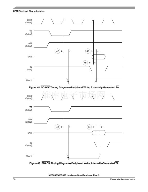
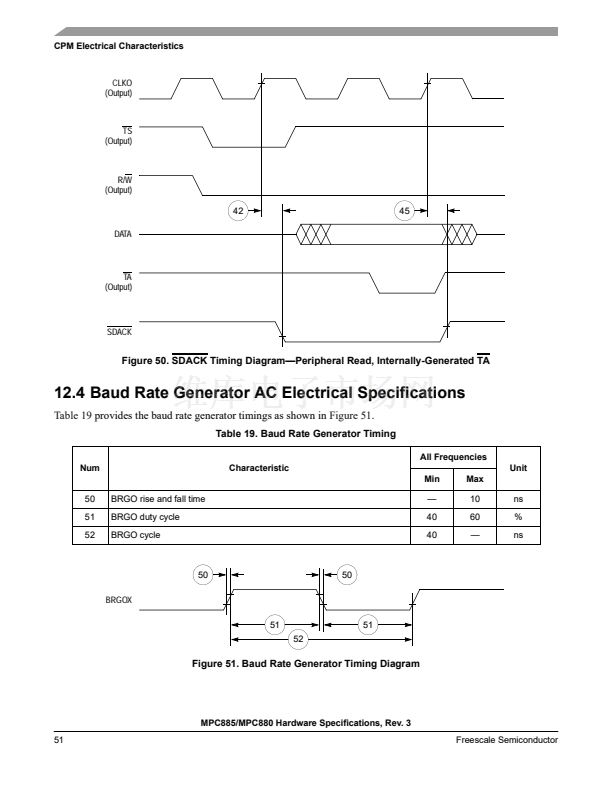
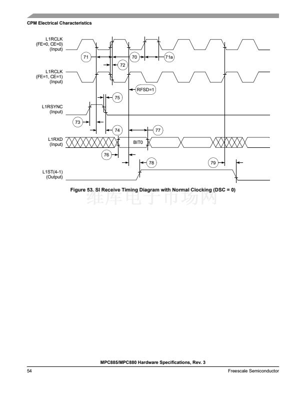
 42
42
 43
43
 44
44
 45
45
 46
46
 47
47
 48
48
 49
49
 50
50
 51
51
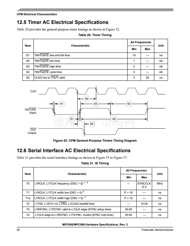 52
52
 53
53
 54
54
 55
55
 56
56
 57
57
 58
58
 59
59
 60
60
 61
61
 62
62
 63
63
 64
64
 65
65
 66
66
 67
67
 68
68
 69
69
 70
70
 71
71
 72
72
 73
73
 74
74
 75
75
 76
76
 77
77
 78
78
 79
79
 80
80
 81
81
 82
82
 83
83
 84
84
 85
85
 86
86
 87
87
 88
88
 89
89
 90
90
 91
91
 92
92
