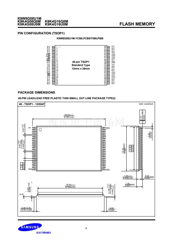
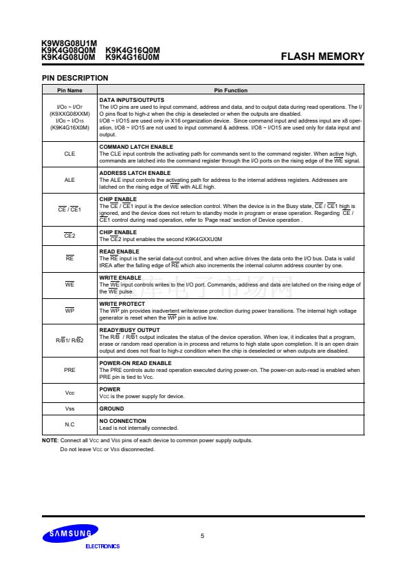
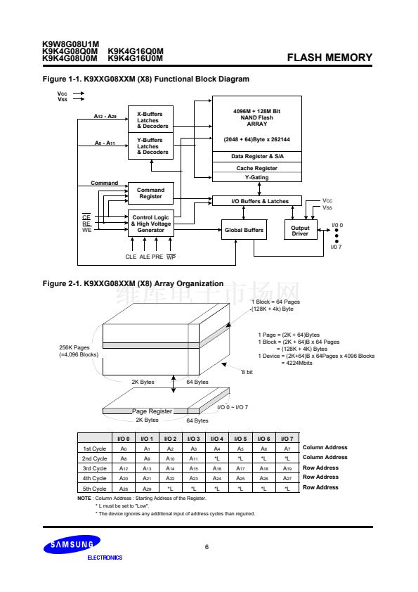
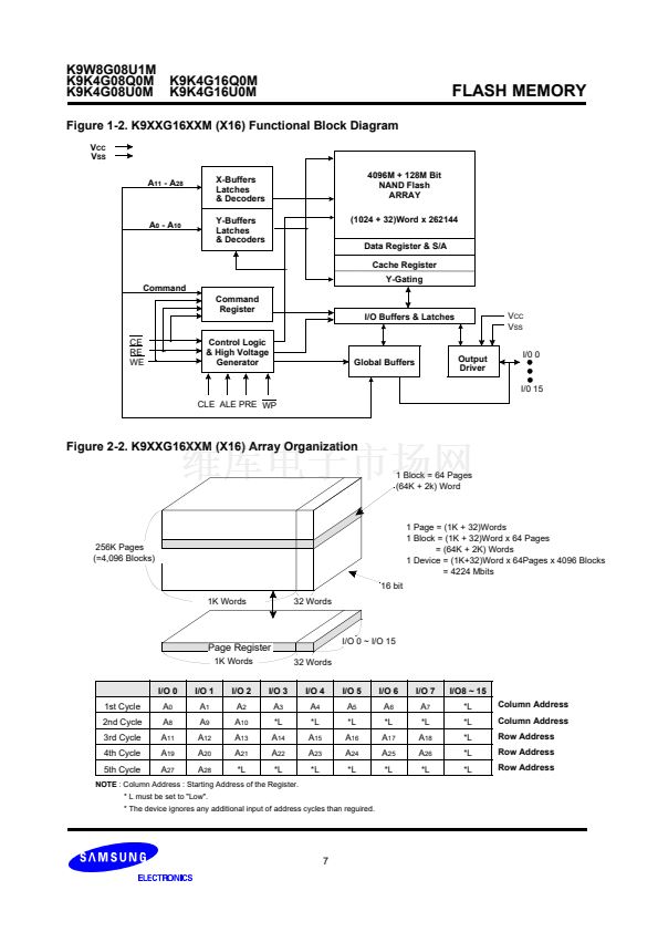
K9W8G08U1M
K9K4G08Q0M
K9K4G08U0M
K9K4G16Q0M
K9K4G16U0M
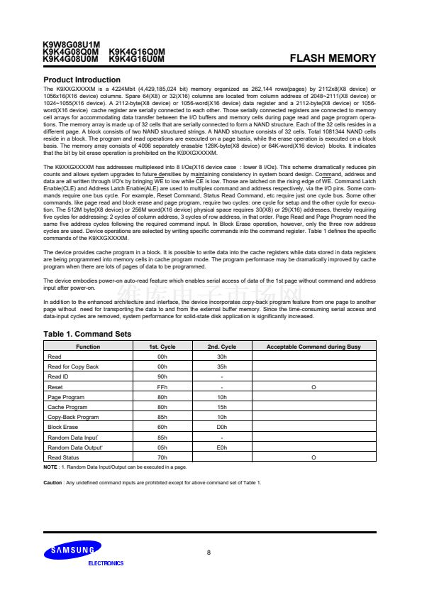
FLASH MEMORY
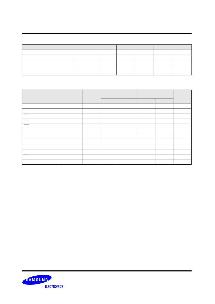
Symbol
t
PROG
t
CBSY
Min
-
Typ
300
3
-
-
-
-
-
2
Max
700
700
4
4
3
Unit
碌s
碌s
cycles
cycles
ms
Program / Erase Characteristics
Parameter
Program Time
Dummy Busy Time for Cache Program
Number of Partial Program Cycles
in the Same Page
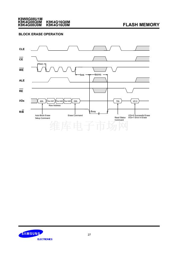
Block Erase Time
Main Array
Spare Array
Nop
t
BERS
NOTE
: 1. Max. time of
t
CBSY
depends on timing between internal program completion and data in
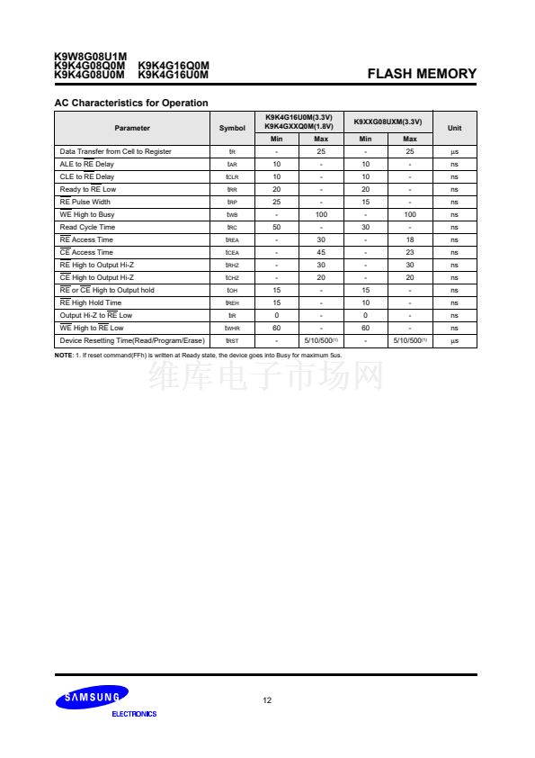
AC Timing Characteristics for Command / Address / Data Input
Parameter
CLE setup Time
CLE Hold Time
CE setup Time
CE Hold Time
WE Pulse Width
ALE setup Time
ALE Hold Time
Data setup Time
Data Hold Time
Write Cycle Time
WE High Hold Time
ALE to Data Loading Time
Symbol
t
CLS
t
CLH
t
CS
t
CH
t
WP
t
ALS
t
ALH
t
DS
t
DH
t
WC
t
WH
t
ADL
K9K4G16U0M(3.3V)
K9K4GXXQ0M(1.8V)
Min
25
10
35
10
25
25
10
20
10
45
15
100
Max
-
-
-
-
-
-
-
-
-
-
-
-
K9XXG08UXM(3.3V)
Min
10
5
15
5
15
10
5
10
5
30
10
100
Max
-
-
-
-
-
-
-
-
-
-
-
-
ns
ns
ns
ns
ns
ns
ns
ns
ns
ns
ns
ns
Unit
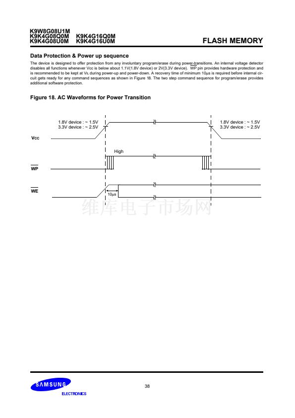
NOTES :
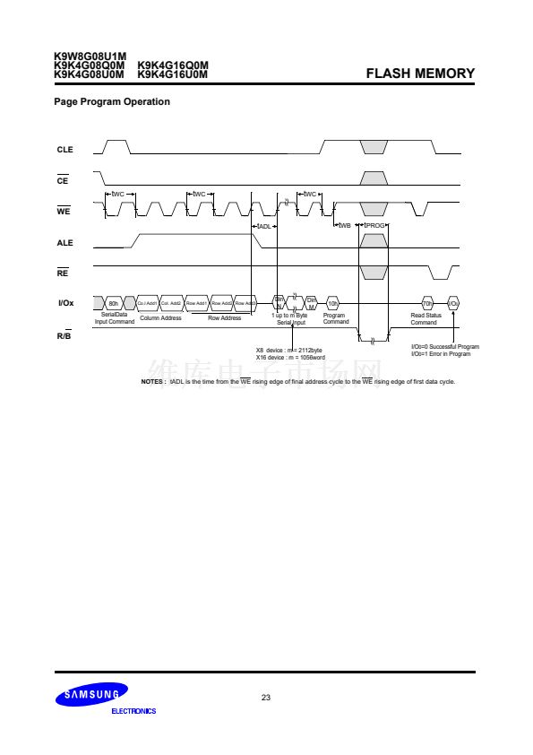
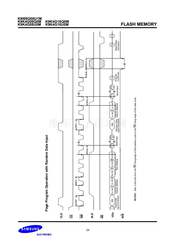
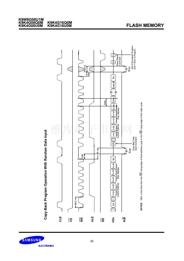
tADL is the time from the WE rising edge of final address cycle to the WE rising edge of first data cycle.
11


 1
1
 2
2
 3
3
 4
4
 5
5
 6
6
 7
7
 8
8
 9
9
 10
10
 11
11
 12
12
 13
13
 14
14
 15
15
 16
16
 17
17
 18
18
 19
19
 20
20
 21
21
 22
22
 23
23
 24
24
 25
25
 26
26
 27
27
 28
28
 29
29
 30
30
 31
31
 32
32
 33
33
 34
34
 35
35
 36
36
 37
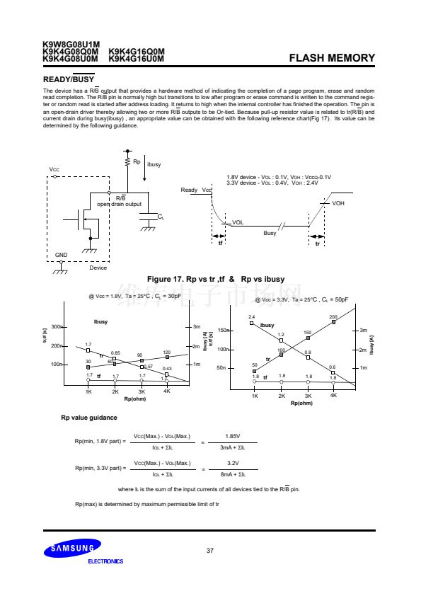
37
 38
38
