K9W8G08U1M
K9K4G08Q0M
K9K4G08U0M
K9K4G16Q0M
K9K4G16U0M
FLASH MEMORY
NAND Flash Technical Notes
(Continued)
Error in write or read operation
Within its life time, additional invalid blocks may develop with NAND Flash memory. Refer to the qualification report for the actual
data.The following possible failure modes should be considered to implement a highly reliable system. In the case of status read fail-
ure after erase or program, block replacement should be done. Because program status fail during a page program does not affect
the data of the other pages in the same block, block replacement can be executed with a page-sized buffer by finding an erased
empty block and reprogramming the current target data and copying the rest of the replaced block.To improve the efficiency of mem-
ory space, it is recommended that the read or verification failure due to single bit error be reclaimed by ECC without any block
replacement. The said additional block failure rate does not include those reclaimed blocks.
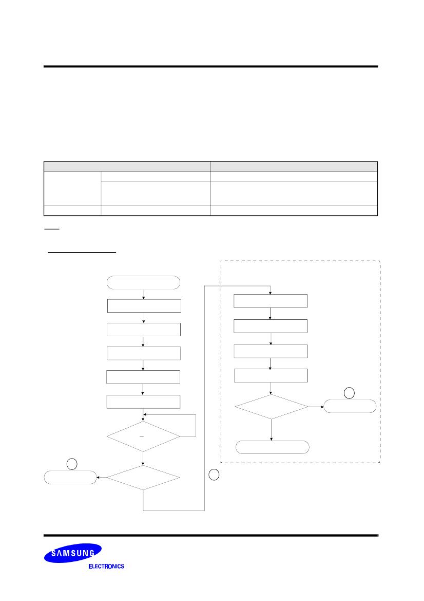
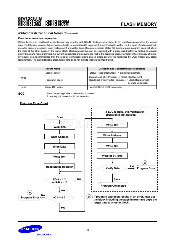
Failure Mode
Erase Failure
Write
Program Failure
Single Bit Failure
Detection and Countermeasure sequence
Status Read after Erase --> Block Replacement
Status Read after Program --> Block Replacement
Read back ( Verify after Program) --> Block Replacement
or ECC Correction
Verify ECC -> ECC Correction
Read
ECC
: Error Correcting Code --> Hamming Code etc.
Example) 1bit correction & 2bit detection
Program Flow Chart
If ECC is used, this verification
operation is not needed.
Start
Write 00h
Write 80h
Write Address
Write Address
Write Data
Write 30h
Write 10h
Wait for tR Time
Read Status Register
Verify Data
Fail
*
Program Error
I/O 6 = 1 ?
or R/B = 1 ?
Yes
No
I/O 0 = 0 ?
No
Pass
Program Completed
*
Program Error
*
: If program operation results in an error, map out
the block including the page in error and copy the
target data to another block.
Yes
14


 1
1
 2
2
 3
3
 4
4
 5
5
 6
6
 7
7
 8
8
 9
9
 10
10
 11
11
 12
12
 13
13
 14
14
 15
15
 16
16
 17
17
 18
18
 19
19
 20
20
 21
21
 22
22
 23
23
 24
24
 25
25
 26
26
 27
27
 28
28
 29
29
 30
30
 31
31
 32
32
 33
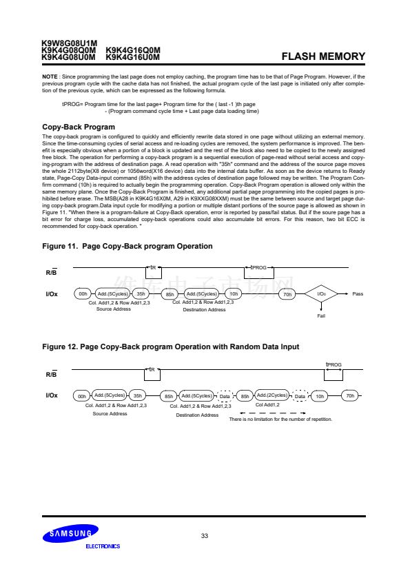
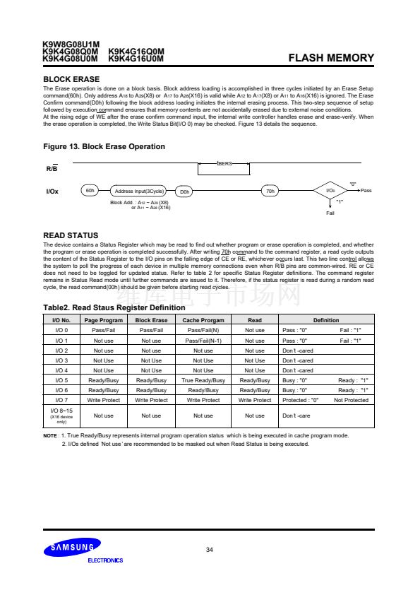
33
 34
34
 35
35
 36
36
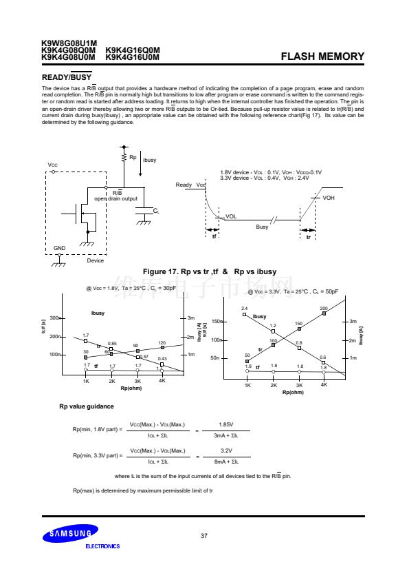 37
37
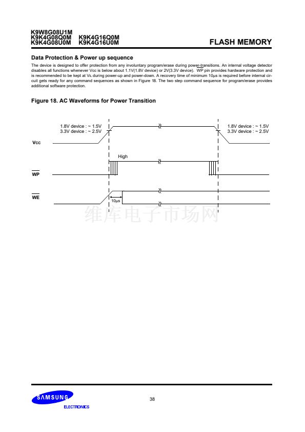 38
38
