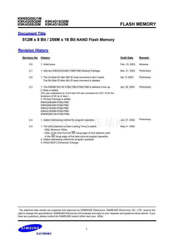
K9W8G08U1M
K9K4G08Q0M
K9K4G08U0M
K9K4G16Q0M
K9K4G16U0M
FLASH MEMORY
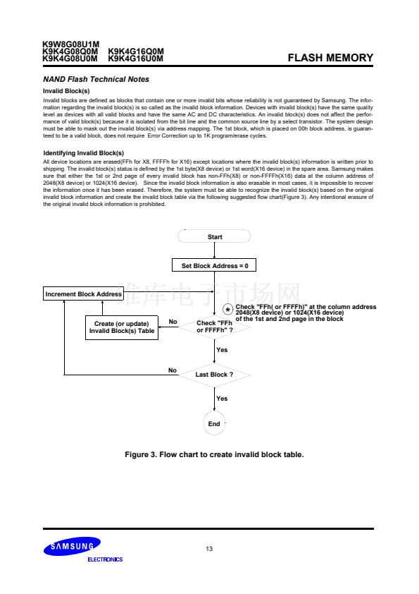
Product Introduction
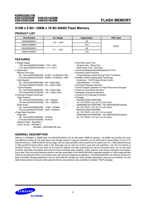
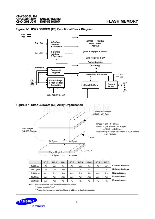
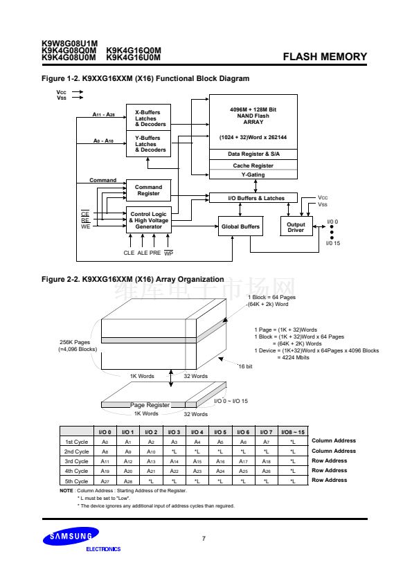
The K9XXGXXXXM is a 4224Mbit (4,429,185,024 bit) memory organized as 262,144 rows(pages) by 2112x8(X8 device) or
1056x16(X16 device) columns. Spare 64(X8) or 32(X16) columns are located from column address of 2048~2111(X8 device) or
1024~1055(X16 device). A 2112-byte(X8 device) or 1056-word(X16 device) data register and a 2112-byte(X8 device) or 1056-
word(X16 device) cache register are serially connected to each other. Those serially connected registers are connected to memory
cell arrays for accommodating data transfer between the I/O buffers and memory cells during page read and page program opera-
tions. The memory array is made up of 32 cells that are serially connected to form a NAND structure. Each of the 32 cells resides in a
different page. A block consists of two NAND structured strings. A NAND structure consists of 32 cells. Total 1081344 NAND cells
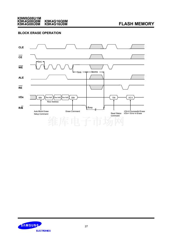
reside in a block. The program and read operations are executed on a page basis, while the erase operation is executed on a block
basis. The memory array consists of 4096 separately erasable 128K-byte(X8 device) or 64K-word(X16 device) blocks. It indicates
that the bit by bit erase operation is prohibited on the K9XXGXXXXM.
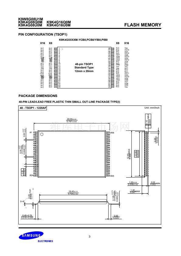
The K9XXGXXXXM has addresses multiplexed into 8 I/Os(X16 device case : lower 8 I/Os). This scheme dramatically reduces pin
counts and allows system upgrades to future densities by maintaining consistency in system board design. Command, address and
data are all written through I/O's by bringing WE to low while CE is low. Those are latched on the rising edge of WE. Command Latch
Enable(CLE) and Address Latch Enable(ALE) are used to multiplex command and address respectively, via the I/O pins. Some com-
mands require one bus cycle. For example, Reset Command, Status Read Command, etc require just one cycle bus. Some other
commands, like page read and block erase and page program, require two cycles: one cycle for setup and the other cycle for execu-
tion. The 512M byte(X8 device) or 256M word(X16 device) physical space requires 30(X8) or 29(X16) addresses, thereby requiring
five cycles for addressing: 2 cycles of column address, 3 cycles of row address, in that order. Page Read and Page Program need the
same five address cycles following the required command input. In Block Erase operation, however, only the three row address
cycles are used. Device operations are selected by writing specific commands into the command register. Table 1 defines the specific
commands of the K9XXGXXXXM.
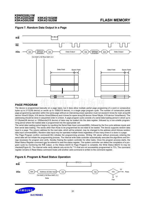
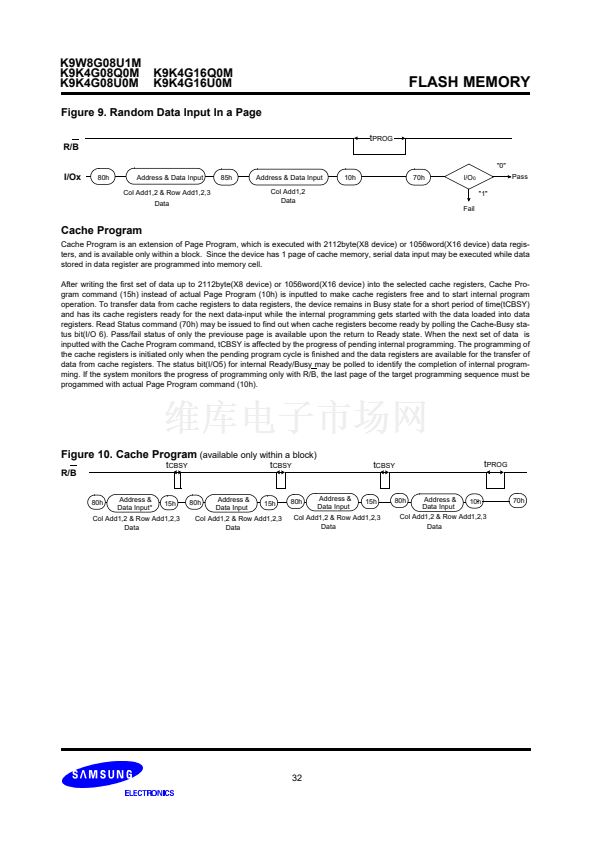
The device provides cache program in a block. It is possible to write data into the cache registers while data stored in data registers
are being programmed into memory cells in cache program mode. The program performace may be dramatically improved by cache
program when there are lots of pages of data to be programmed.
The device embodies power-on auto-read feature which enables serial access of data of the 1st page without command and address
input after power-on.
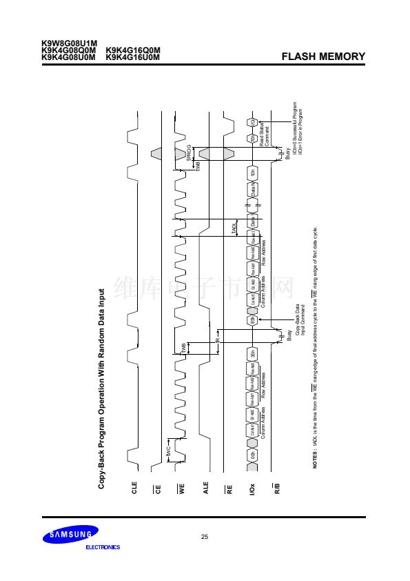
In addition to the enhanced architecture and interface, the device incorporates copy-back program feature from one page to another
page without need for transporting the data to and from the external buffer memory. Since the time-consuming serial access and
data-input cycles are removed, system performance for solid-state disk application is significantly increased.
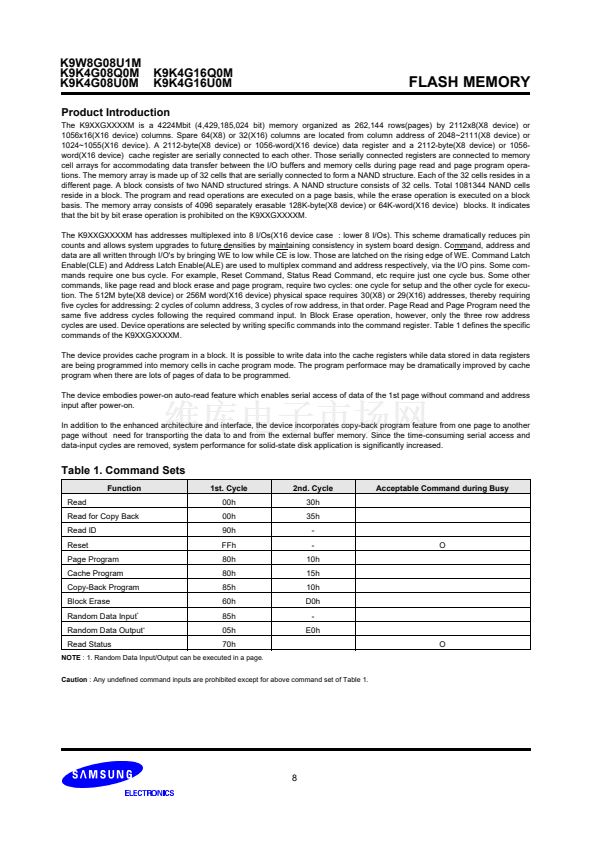
Table 1. Command Sets
Function
Read
Read for Copy Back
Read ID
Reset
Page Program
Cache Program
Copy-Back Program
Block Erase
Random Data Input
*
Random Data Output
*
Read Status
1st. Cycle
00h
00h
90h
FFh
80h
80h
85h
60h
85h
05h
70h
2nd. Cycle
30h
35h
-
-
10h
15h
10h
D0h
-
E0h
O
O
Acceptable Command during Busy
NOTE
: 1. Random Data Input/Output can be executed in a page.
Caution
: Any undefined command inputs are prohibited except for above command set of Table 1.
8


 1
1
 2
2
 3
3
 4
4
 5
5
 6
6
 7
7
 8
8
 9
9
 10
10
 11
11
 12
12
 13
13
 14
14
 15
15
 16
16
 17
17
 18
18
 19
19
 20
20
 21
21
 22
22
 23
23
 24
24
 25
25
 26
26
 27
27
 28
28
 29
29
 30
30
 31
31
 32
32
 33
33
 34
34
 35
35
 36
36
 37
37
 38
38
