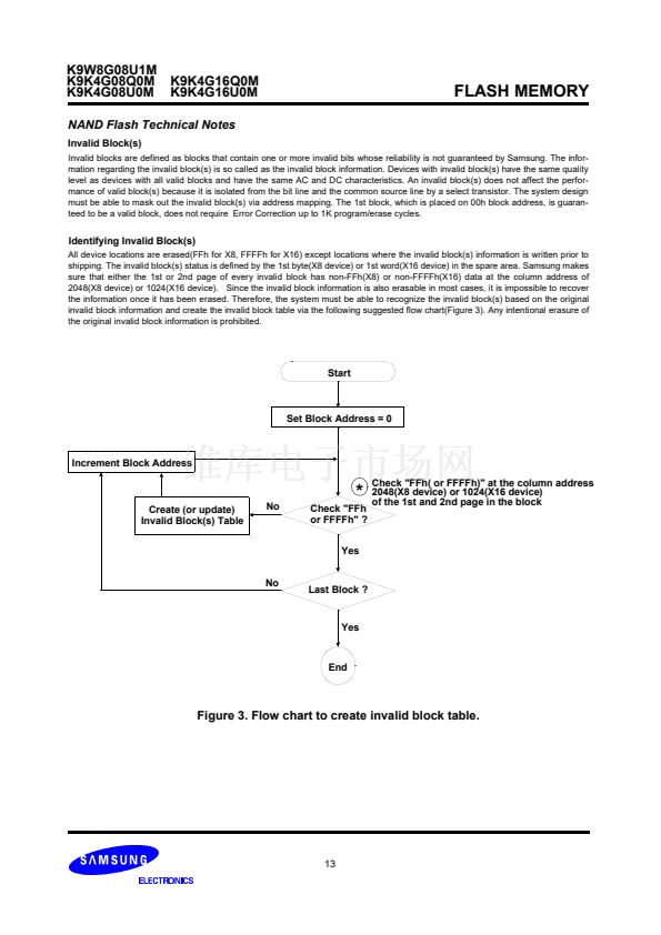
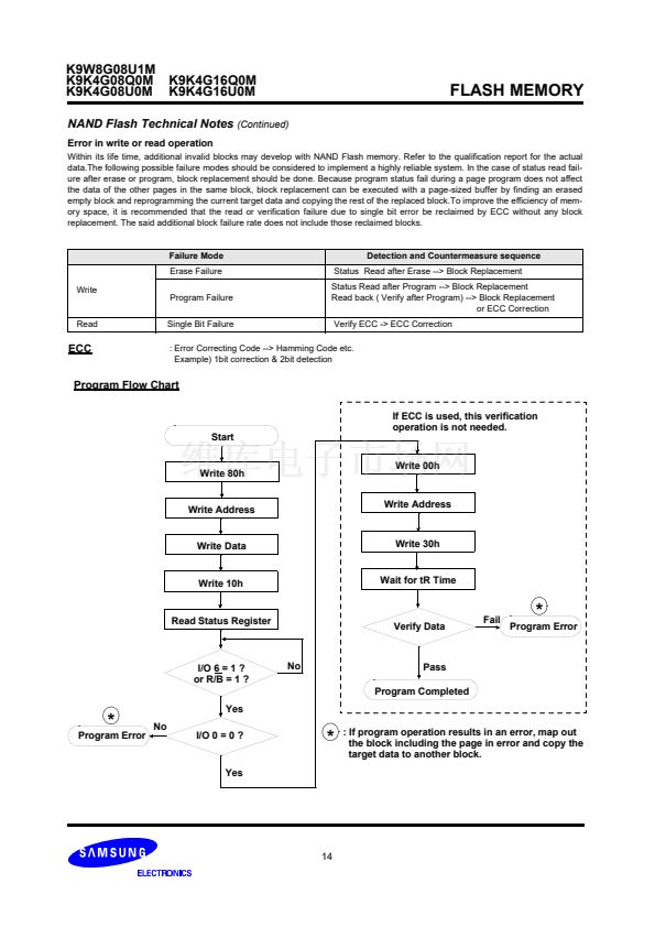
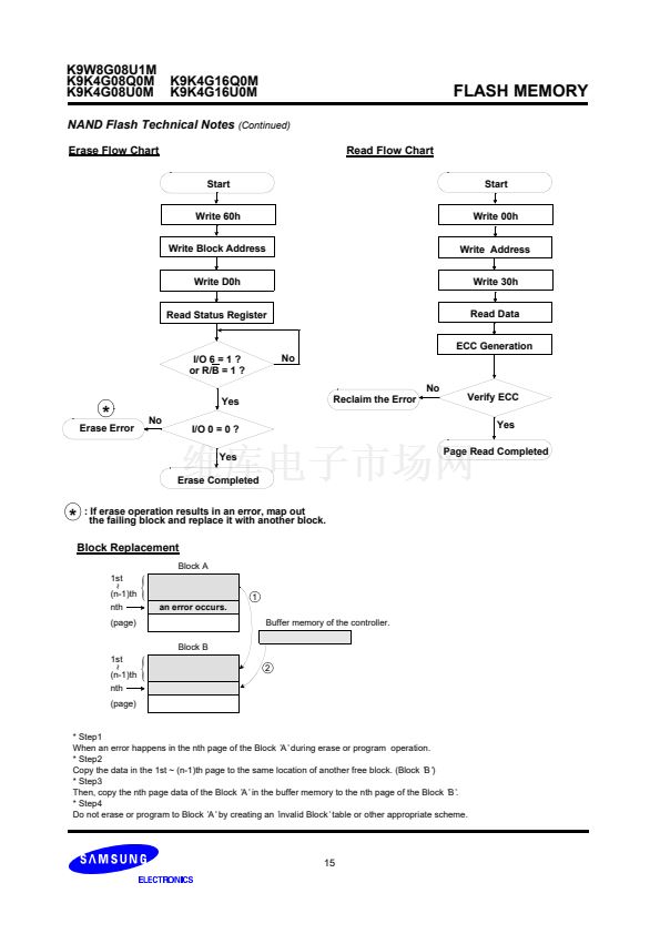
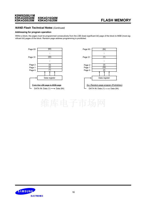
K9W8G08U1M
K9K4G08Q0M
K9K4G08U0M
K9K4G16Q0M
K9K4G16U0M
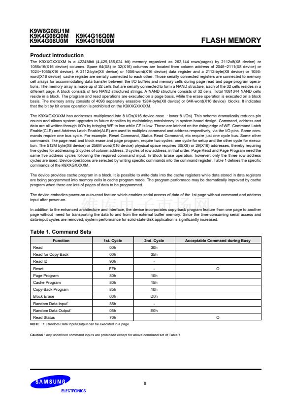
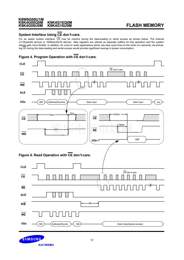
FLASH MEMORY
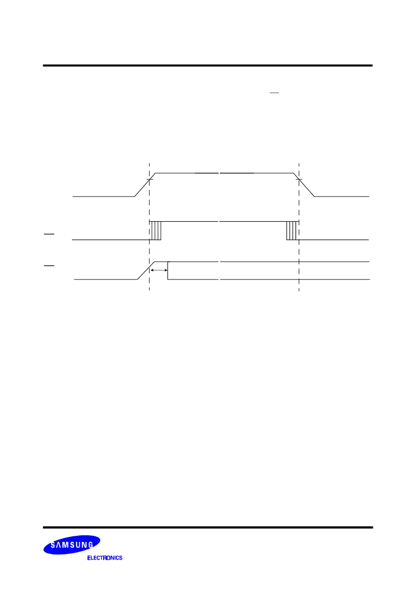
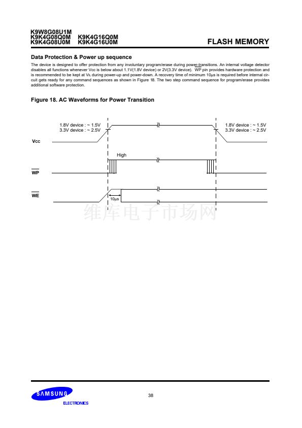
Data Protection & Power up sequence
The device is designed to offer protection from any involuntary program/erase during power-transitions. An internal voltage detector
disables all functions whenever Vcc is below about 1.1V(1.8V device) or 2V(3.3V device). WP pin provides hardware protection and
is recommended to be kept at V
IL
during power-up and power-down. A recovery time of minimum 10碌s is required before internal cir-
cuit gets ready for any command sequences as shown in Figure 18. The two step command sequence for program/erase provides
additional software protection.
Figure 18. AC Waveforms for Power Transition
1.8V device : ~ 1.5V
3.3V device : ~ 2.5V
V
CC
High
鈮?/div>
1.8V device : ~ 1.5V
3.3V device : ~ 2.5V
WP
WE
38


 1
1
 2
2
 3
3
 4
4
 5
5
 6
6
 7
7
 8
8
 9
9
 10
10
 11
11
 12
12
 13
13
 14
14
 15
15
 16
16
 17
17
 18
18
 19
19
 20
20
 21
21
 22
22
 23
23
 24
24
 25
25
 26
26
 27
27
 28
28
 29
29
 30
30
 31
31
 32
32
 33
33
 34
34
 35
35
 36
36
 37
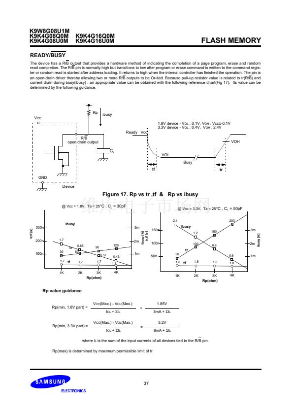
37
 38
38
