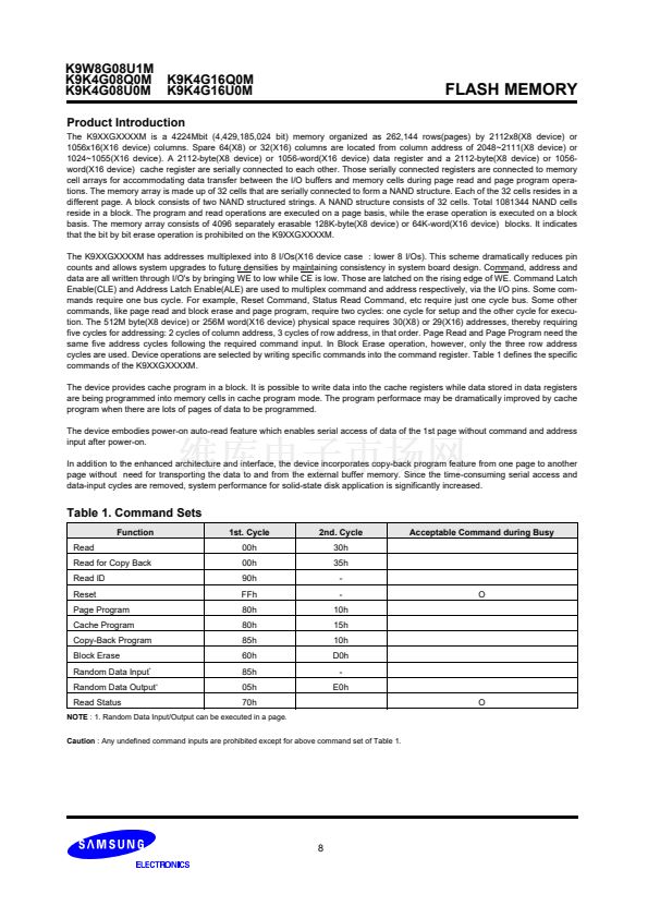
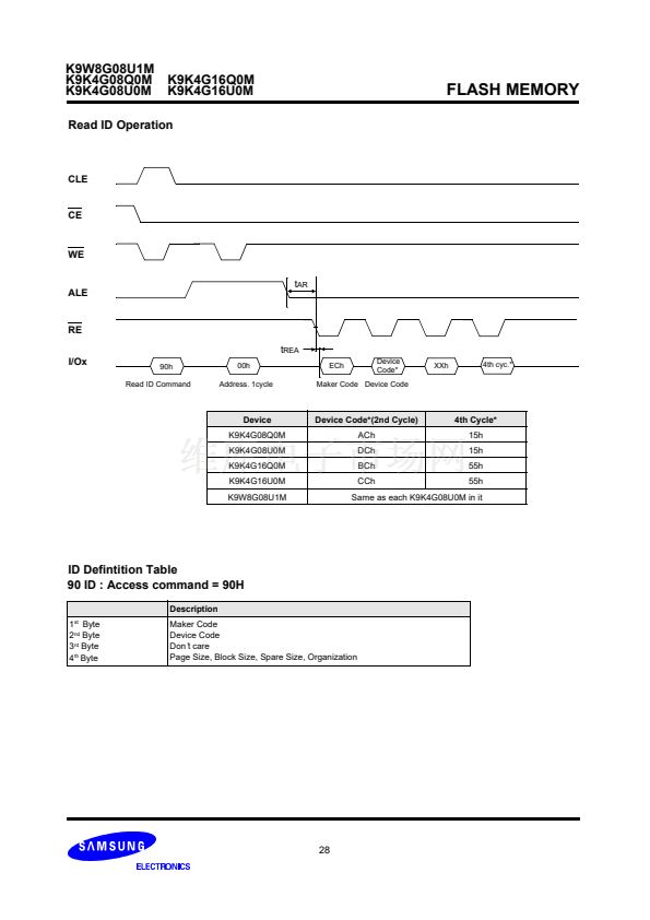
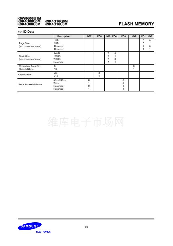
K9W8G08U1M
K9K4G08Q0M
K9K4G08U0M
K9K4G16Q0M
K9K4G16U0M
FLASH MEMORY
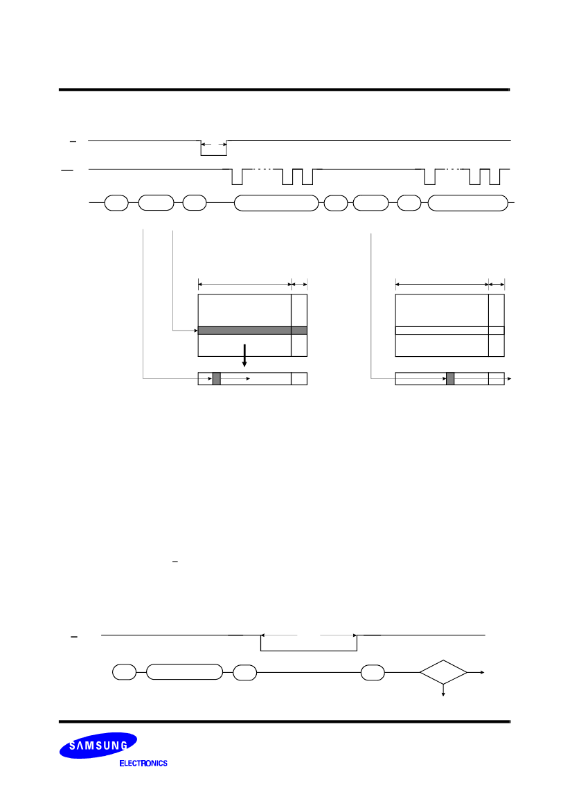
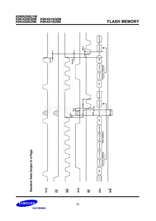
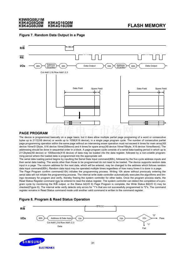
Figure 7. Random Data Output In a Page
R/B
RE
I/Ox
00h
Address
5Cycles
30h
t
R
Data Output
05h
Address
2Cycles
E0h
Data Output
Col Add1,2 & Row Add1,2,3
Data Field
Spare Field
Data Field
Spare Field
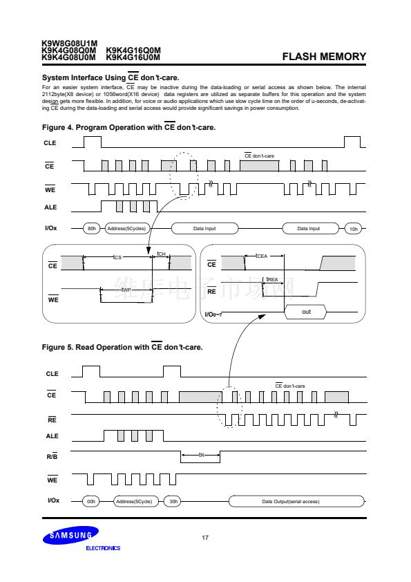
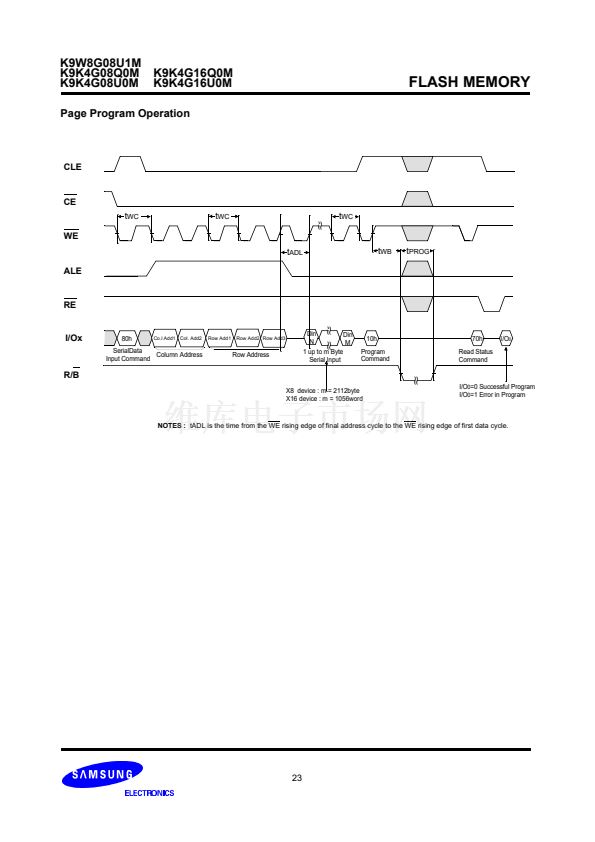
PAGE PROGRAM
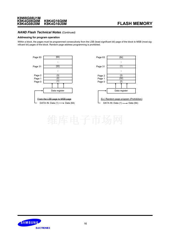
The device is programmed basically on a page basis, but it does allow multiple partial page programing of a word or consecutive
bytes up to 2112(X8 device) or words up to 1056(X16 device), in a single page program cycle. The number of consecutive partial
page programming operation within the same page without an intervening erase operation must not exceed 4 times for main array(X8
device:1time/512byte, X16 device:1time/256word) and 4 times for spare array(X8 device:1time/16byte, X16 device:1time/8word). The
addressing should be done in sequential order in a block. A page program cycle consists of a serial data loading period in which up to
2112bytes(X8 device) or 1056words(X16 device) of data may be loaded into the data register, followed by a non-volatile program-
ming period where the loaded data is programmed into the appropriate cell.
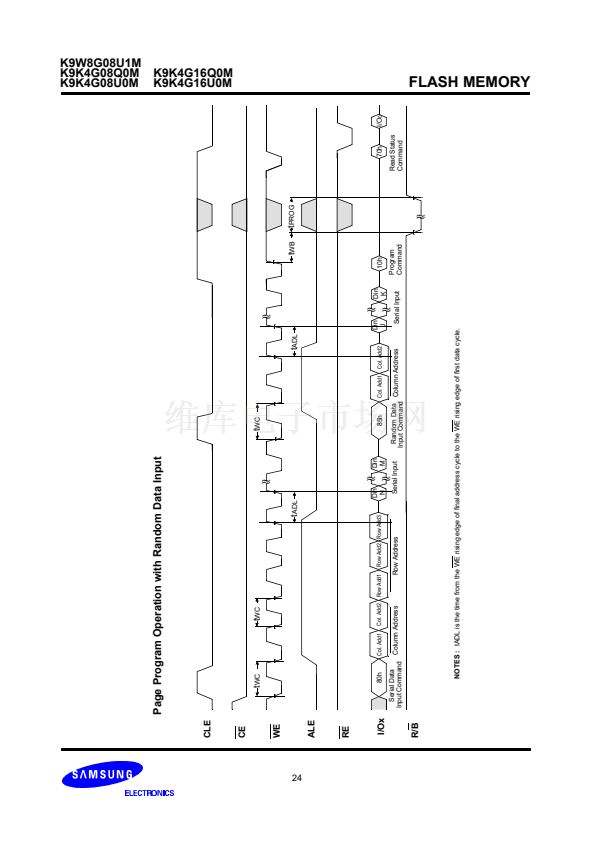
The serial data loading period begins by inputting the Serial Data Input command(80h), followed by the five cycle address inputs and
then serial data loading. The words other than those to be programmed do not need to be loaded. The device supports random data
input in a page. The column address for the next data, which will be entered, may be changed to the address which follows random
data input command(85h). Random data input may be operated multiple times regardless of how many times it is done in a page.
The Page Program confirm command(10h) initiates the programming process. Writing 10h alone without previously entering the
serial data will not initiate the programming process. The internal write state controller automatically executes the algorithms and tim-
ings necessary for program and verify, thereby freeing the system controller for other tasks. Once the program process starts, the
Read Status Register command may be entered to read the status register. The system controller can detect the completion of a pro-
gram cycle by monitoring the R/B output, or the Status bit(I/O 6) Page Program is complete, the Write Status Bit(I/O 0) may be
checked(Figure 8). The internal write verify detects only errors for "1"s that are not successfully programmed to "0"s. The command
register remains in Read Status command mode until another valid command is written to the command register.
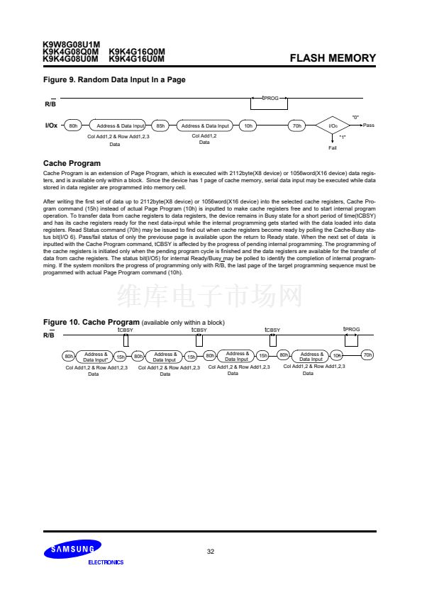
Figure 8. Program & Read Status Operation
t
PROG
R/B
"0"
I/Ox
80h
Address & Data Input
Col Add1,2 & Row Add1,2,3
Data
10h
70h
I/O
0
"1"
Fail
Pass
31


 1
1
 2
2
 3
3
 4
4
 5
5
 6
6
 7
7
 8
8
 9
9
 10
10
 11
11
 12
12
 13
13
 14
14
 15
15
 16
16
 17
17
 18
18
 19
19
 20
20
 21
21
 22
22
 23
23
 24
24
 25
25
 26
26
 27
27
 28
28
 29
29
 30
30
 31
31
 32
32
 33
33
 34
34
 35
35
 36
36
 37
37
 38
38
