鈥?/div>
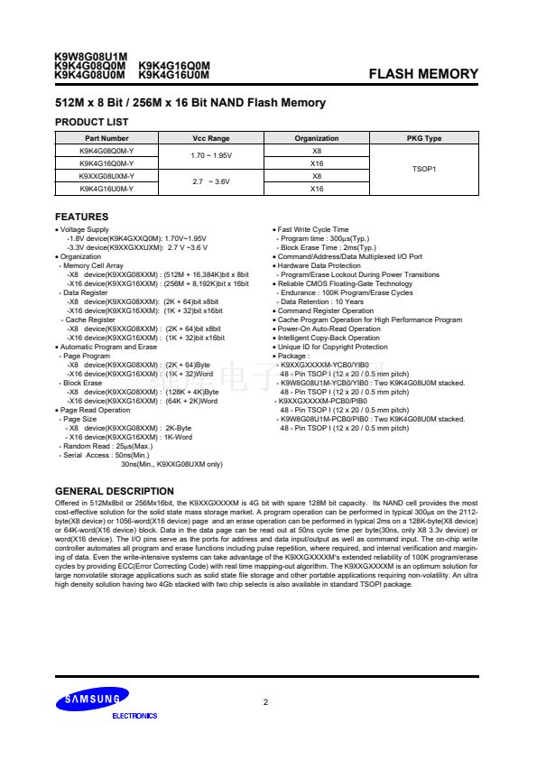
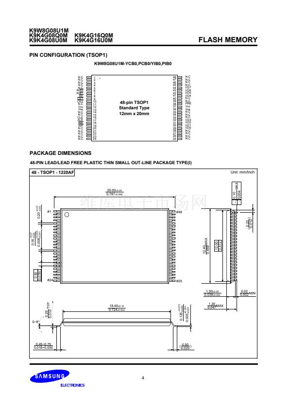
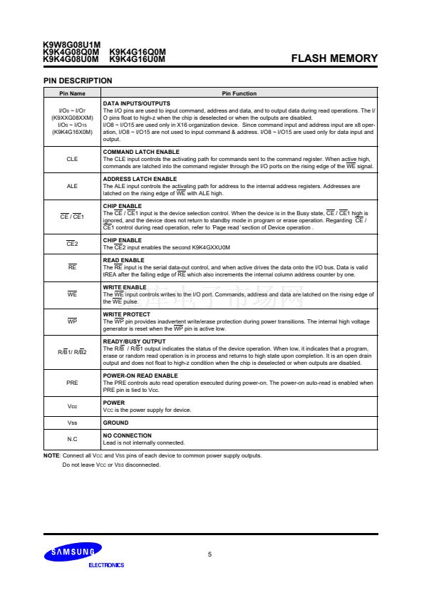
Package :
- K9XXGXXXXM-YCB0/YIB0
48 - Pin TSOP I (12 x 20 / 0.5 mm pitch)
- K9W8G08U1M-YCB0/YIB0 : Two K9K4G08U0M stacked.
48 - Pin TSOP I (12 x 20 / 0.5 mm pitch)
- K9XXGXXXXM-PCB0/PIB0
48 - Pin TSOP I (12 x 20 / 0.5 mm pitch)
- K9W8G08U1M-PCB0/PIB0 : Two K9K4G08U0M stacked.
48 - Pin TSOP I (12 x 20 / 0.5 mm pitch)
GENERAL DESCRIPTION
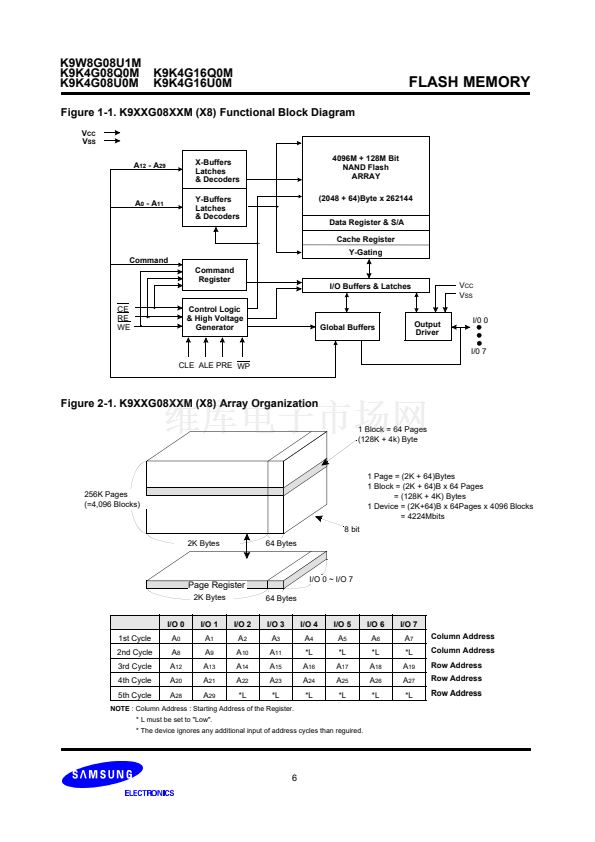
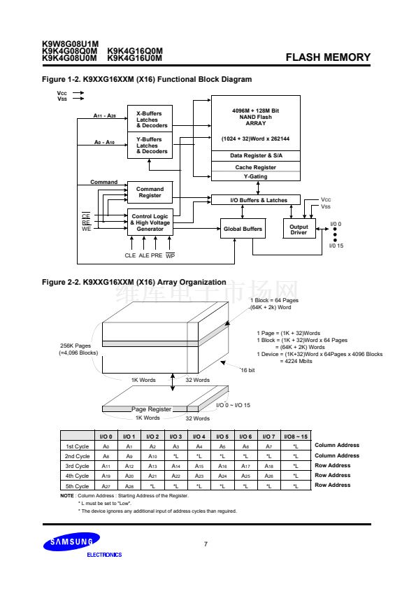
Offered in 512Mx8bit or 256Mx16bit, the K9XXGXXXXM is 4G bit with spare 128M bit capacity. Its NAND cell provides the most
cost-effective solution for the solid state mass storage market. A program operation can be performed in typical 300碌s on the 2112-
byte(X8 device) or 1056-word(X16 device) page and an erase operation can be performed in typical 2ms on a 128K-byte(X8 device)
or 64K-word(X16 device) block. Data in the data page can be read out at 50ns cycle time per byte(30ns, only X8 3.3v device) or
word(X16 device). The I/O pins serve as the ports for address and data input/output as well as command input. The on-chip write
controller automates all program and erase functions including pulse repetition, where required, and internal verification and margin-
ing of data. Even the write-intensive systems can take advantage of the K9XXGXXXXM鈥瞫 extended reliability of 100K program/erase
cycles by providing ECC(Error Correcting Code) with real time mapping-out algorithm. The K9XXGXXXXM is an optimum solution for
large nonvolatile storage applications such as solid state file storage and other portable applications requiring non-volatility. An ultra
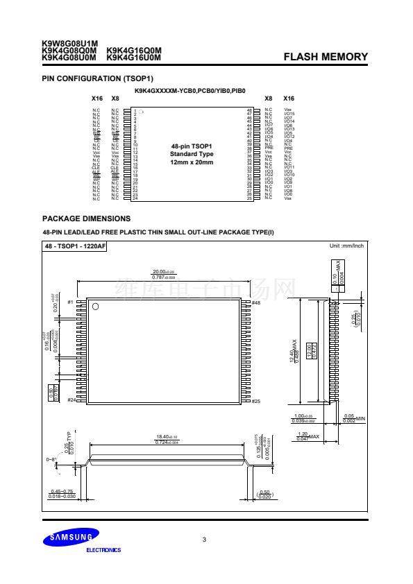
high density solution having two 4Gb stacked with two chip selects is also available in standard TSOPI package.
2


 1
1
 2
2
 3
3
 4
4
 5
5
 6
6
 7
7
 8
8
 9
9
 10
10
 11
11
 12
12
 13
13
 14
14
 15
15
 16
16
 17
17
 18
18
 19
19
 20
20
 21
21
 22
22
 23
23
 24
24
 25
25
 26
26
 27
27
 28
28
 29
29
 30
30
 31
31
 32
32
 33
33
 34
34
 35
35
 36
36
 37
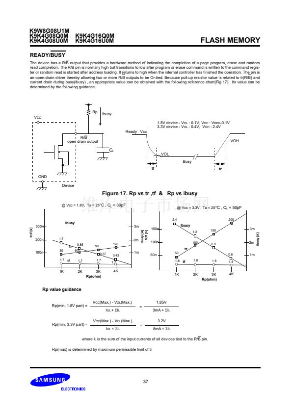
37
 38
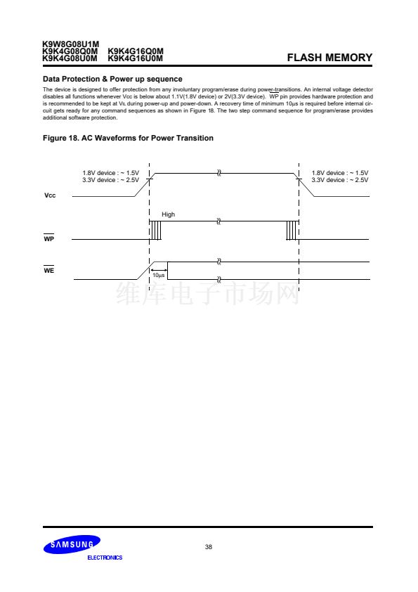
38
