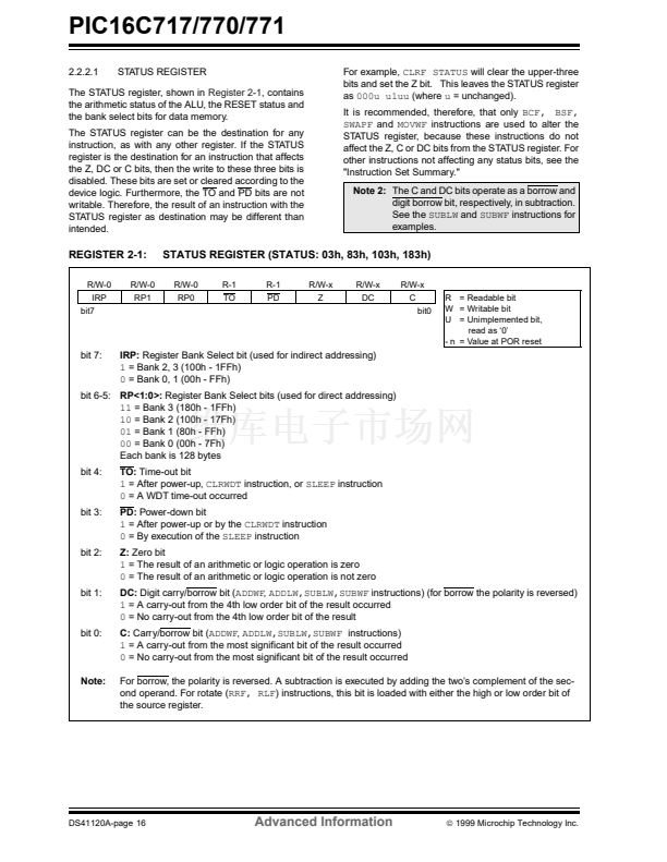
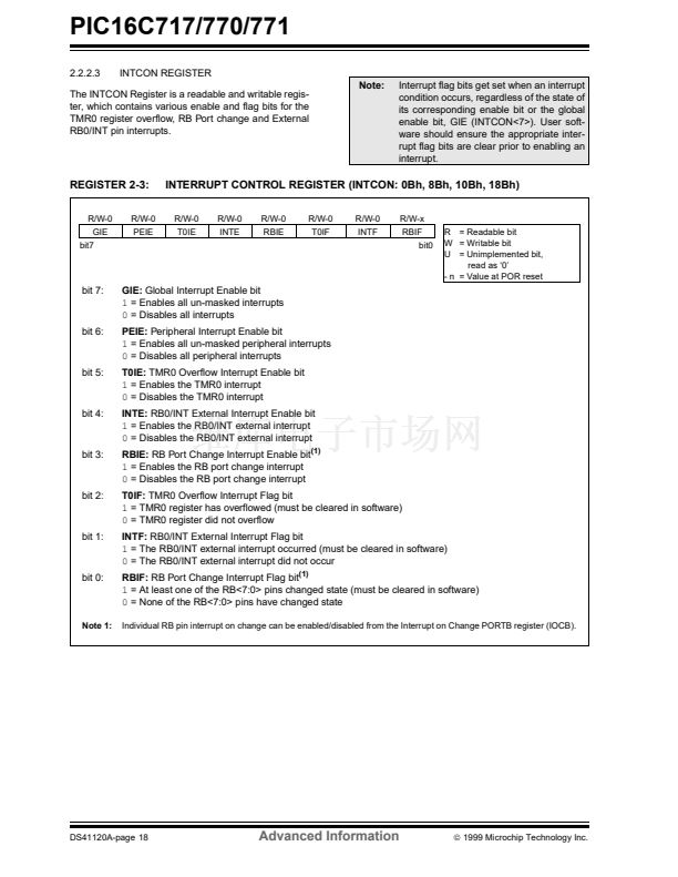
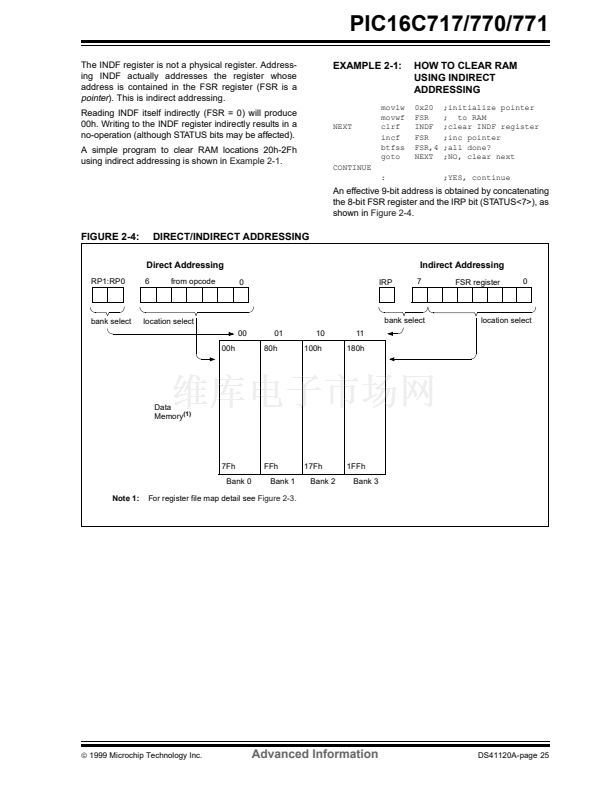
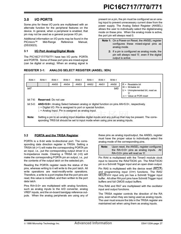
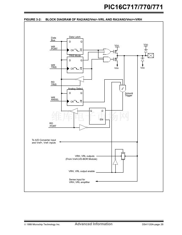
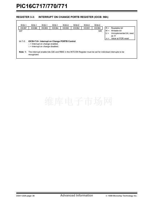
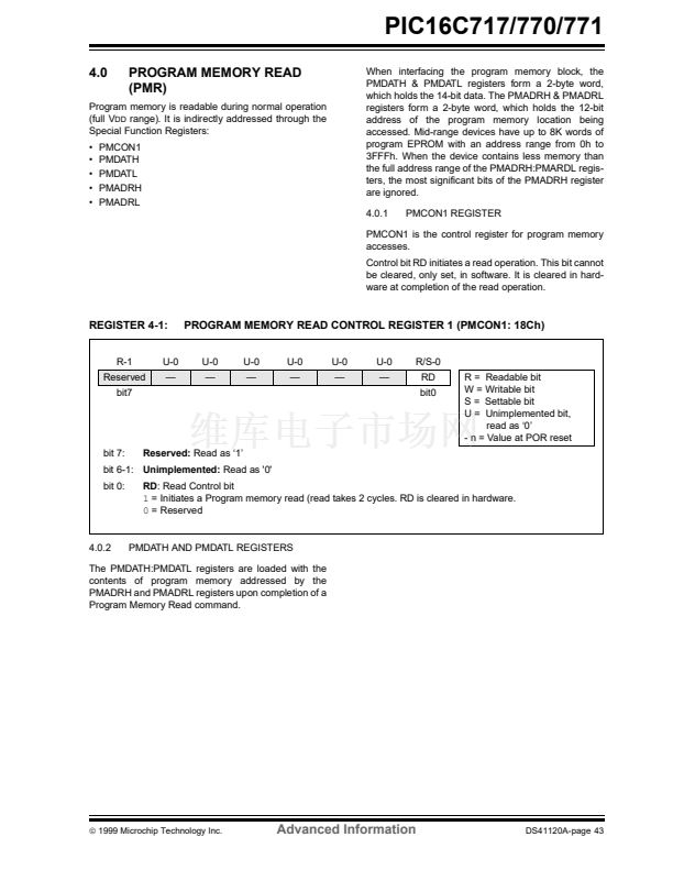
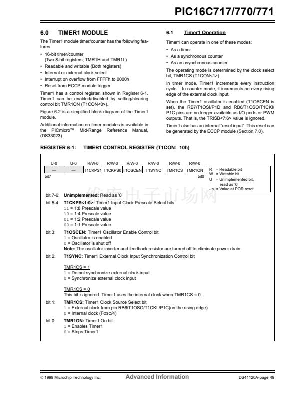
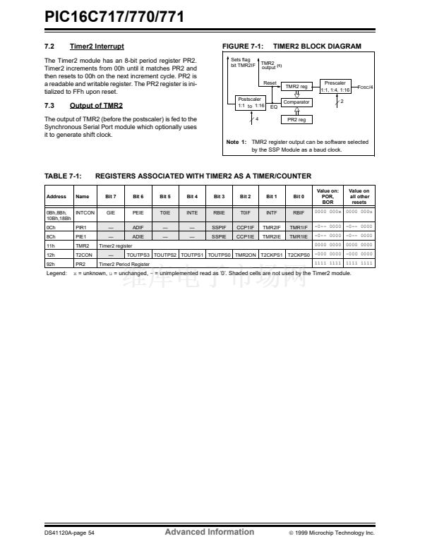
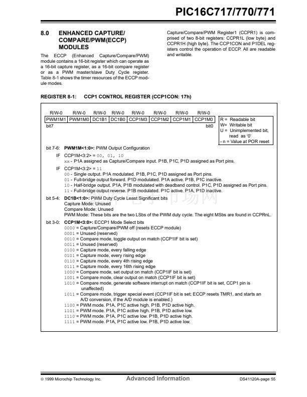
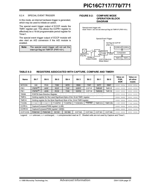
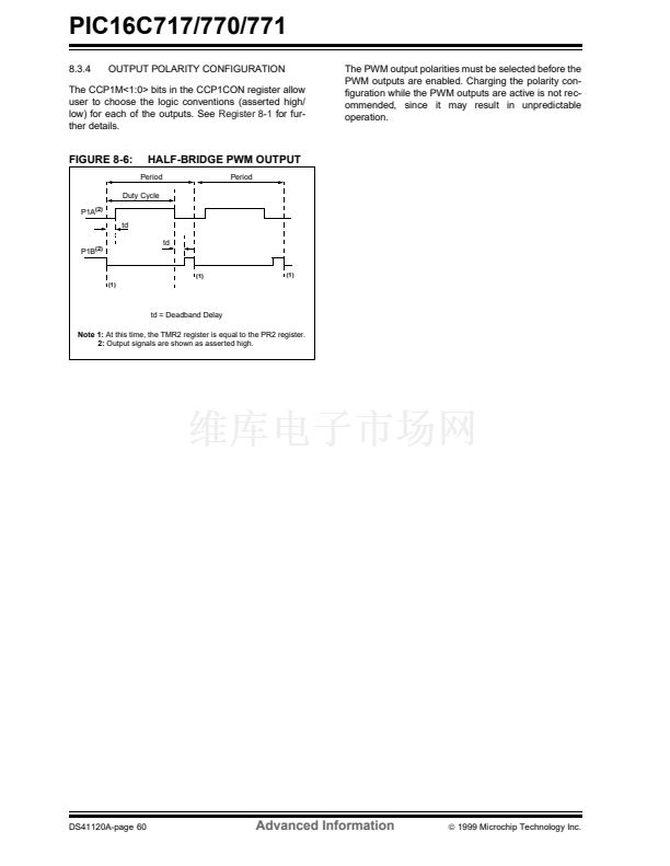
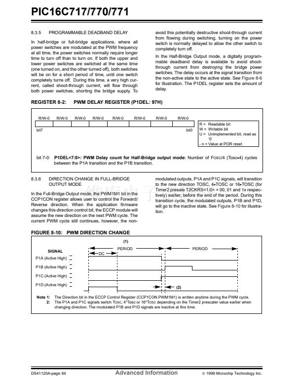
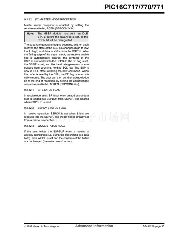
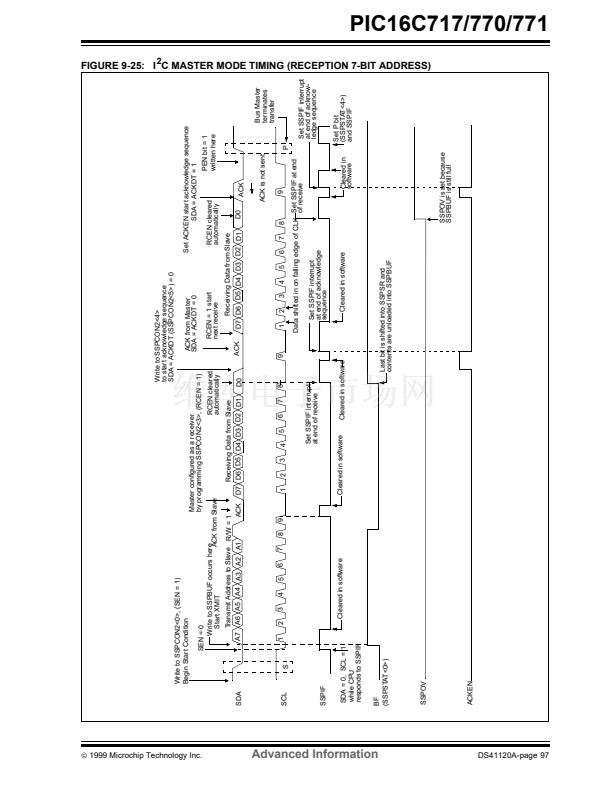
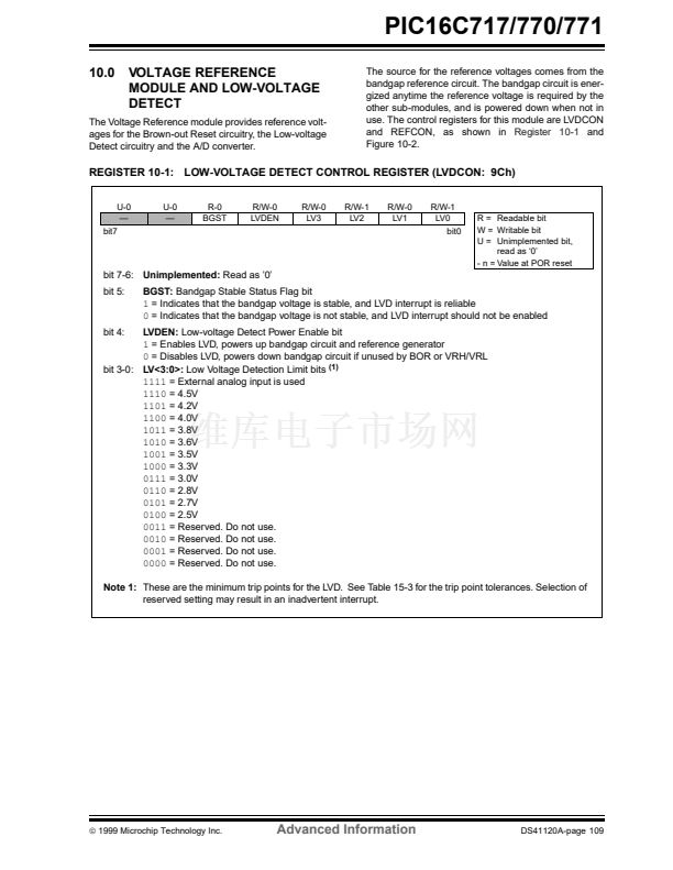
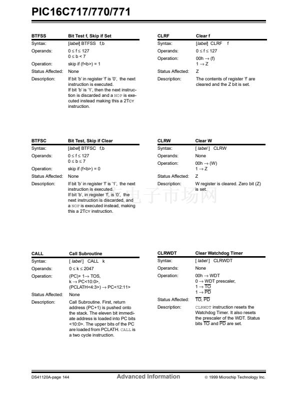
PIC16C717/770/771
5.2.1
SWITCHING PRESCALER ASSIGNMENT
5.3
Timer0 Interrupt
The prescaler assignment is fully under software con-
trol, i.e., it can be changed 鈥渙n-the-fly鈥?during program
execution.
Note:
To avoid an unintended device RESET, a
specific instruction sequence (shown in the
PICmicro鈩?Mid-Range Reference Man-
ual, DS33023) must be executed when
changing the prescaler assignment from
Timer0 to the WDT. This sequence must
be followed even if the WDT is disabled.
The TMR0 interrupt is generated when the TMR0 reg-
ister overflows from FFh to 00h. This overflow sets bit
T0IF (INTCON<2>). The interrupt can be masked by
clearing bit T0IE (INTCON<5>). Bit T0IF must be
cleared in software by the Timer0 module interrupt ser-
vice routine before re-enabling this interrupt. The
TMR0 interrupt cannot awaken the processor from
SLEEP since the timer is shut off during SLEEP.
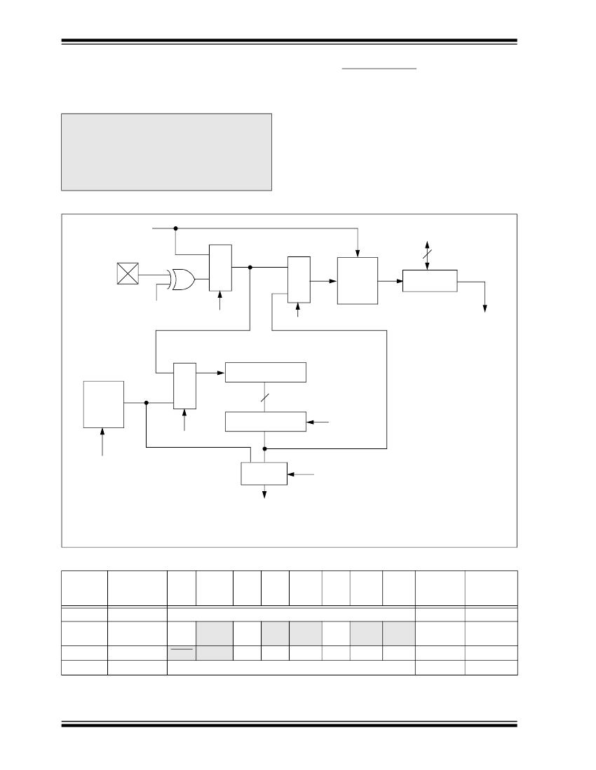
FIGURE 5-2:
BLOCK DIAGRAM OF THE TIMER0/WDT PRESCALER
Data Bus
8
1
0
M
U
X
SYNC
2
Cycles
TMR0 reg
CLKOUT (= F
OSC
/4)
0
RA4/T0CKI
Pin
1
T0SE
M
U
X
T0CS
PSA
Set flag bit T0IF
on Overflow
0
M
U
X
8-bit Prescaler
8
8 - to - 1MUX
PS<2:0>
Watchdog
Timer
1
PSA
0
MUX
1
PSA
WDT Enable Bit
WDT
Time-out
Note:
T0CS, T0SE, PSA, PS<2:0> are (OPTION_REG<5:0>).
TABLE 5-1:
Address
01h,101h
0Bh,8Bh,
10Bh,18Bh
81h,181h
85h
REGISTERS ASSOCIATED WITH TIMER0
Bit 7
Bit 6
Bit 5
Bit 4
Bit 3
Bit 2
Bit 1
Bit 0
Value on:
POR,
BOR
xxxx xxxx
T0IE
T0CS
INTE
T0SE
RBIE
PSA
T0IF
PS2
INTF
PS1
RBIF
PS0
0000 000x
1111 1111
1111 1111
Value on all
other resets
uuuu uuuu
0000 000u
1111 1111
1111 1111
Name
TMR0
INTCON
OPTION_REG
TRISA
Timer0 register
GIE
PEIE
RBPU INTEDG
PORTA Data Direction Register
Legend:
x
= unknown,
u
= unchanged,
-
= unimplemented locations read as 鈥?鈥? Shaded cells are not used by Timer0.
DS41120A-page 48
Advanced Information
漏
1999 Microchip Technology Inc.


 1
1
 2
2
 3
3
 4
4
 5
5
 6
6
 7
7
 8
8
 9
9
 10
10
 11
11
 12
12
 13
13
 14
14
 15
15
 16
16
 17
17
 18
18
 19
19
 20
20
 21
21
 22
22
 23
23
 24
24
 25
25
 26
26
 27
27
 28
28
 29
29
 30
30
 31
31
 32
32
 33
33
 34
34
 35
35
 36
36
 37
37
 38
38
 39
39
 40
40
 41
41
 42
42
 43
43
 44
44
 45
45
 46
46
 47
47
 48
48
 49
49
 50
50
 51
51
 52
52
 53
53
 54
54
 55
55
 56
56
 57
57
 58
58
 59
59
 60
60
 61
61
 62
62
 63
63
 64
64
 65
65
 66
66
 67
67
 68
68
 69
69
 70
70
 71
71
 72
72
 73
73
 74
74
 75
75
 76
76
 77
77
 78
78
 79
79
 80
80
 81
81
 82
82
 83
83
 84
84
 85
85
 86
86
 87
87
 88
88
 89
89
 90
90
 91
91
 92
92
 93
93
 94
94
 95
95
 96
96
 97
97
 98
98
 99
99
 100
100
 101
101
 102
102
 103
103
 104
104
 105
105
 106
106
 107
107
 108
108
 109
109
 110
110
 111
111
 112
112
 113
113
 114
114
 115
115
 116
116
 117
117
 118
118
 119
119
 120
120
 121
121
 122
122
 123
123
 124
124
 125
125
 126
126
 127
127
 128
128
 129
129
 130
130
 131
131
 132
132
 133
133
 134
134
 135
135
 136
136
 137
137
 138
138
 139
139
 140
140
 141
141
 142
142
 143
143
 144
144
 145
145
 146
146
 147
147
 148
148
 149
149
 150
150
 151
151
 152
152
 153
153
 154
154
 155
155
 156
156
 157
157
 158
158
 159
159
 160
160
 161
161
 162
162
 163
163
 164
164
 165
165
 166
166
 167
167
 168
168
 169
169
 170
170
 171
171
 172
172
 173
173
 174
174
 175
175
 176
176
 177
177
 178
178
 179
179
 180
180
 181
181
 182
182
 183
183
 184
184
 185
185
 186
186
 187
187
 188
188
 189
189
 190
190
 191
191
 192
192
 193
193
 194
194
 195
195
 196
196
 197
197
 198
198
 199
199
 200
200
