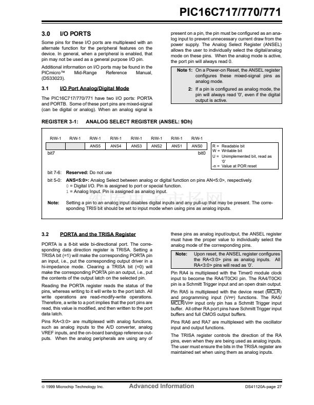
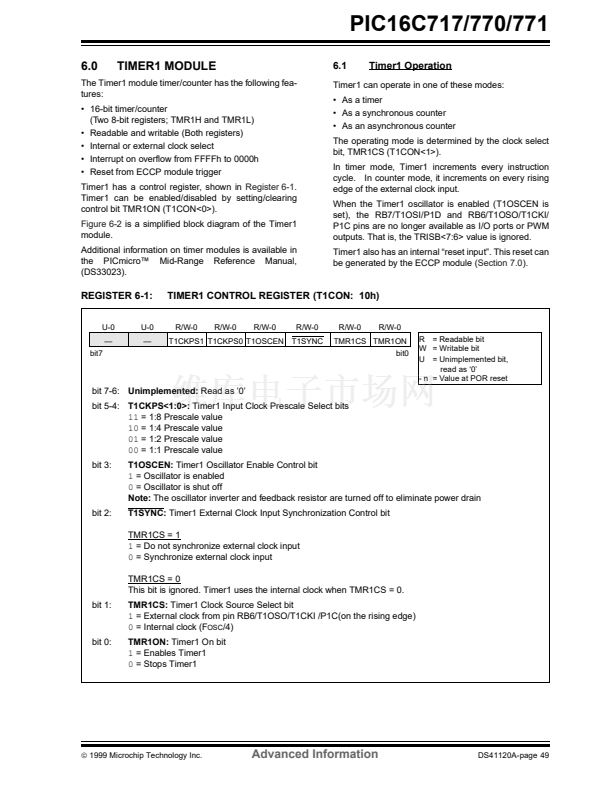
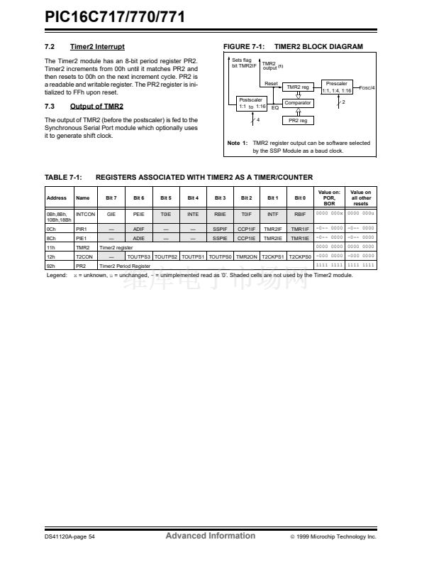
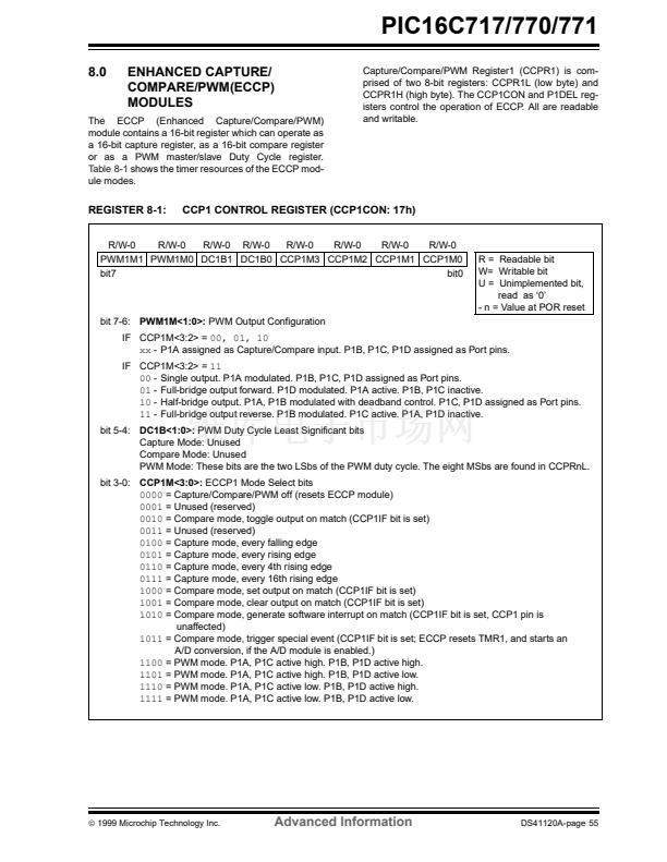
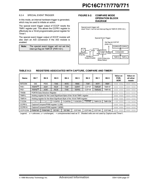
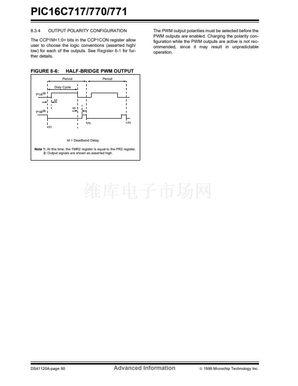
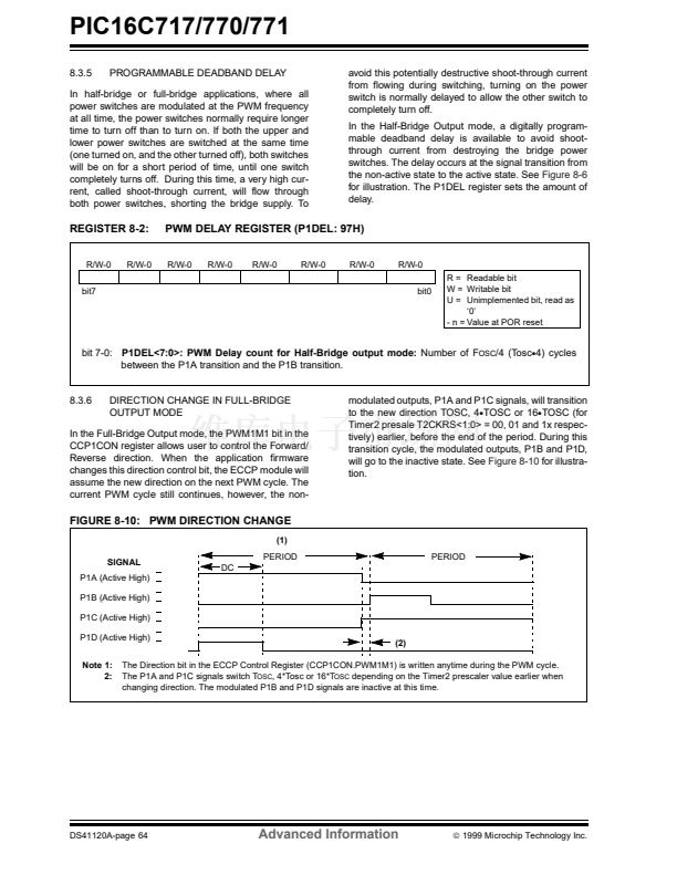
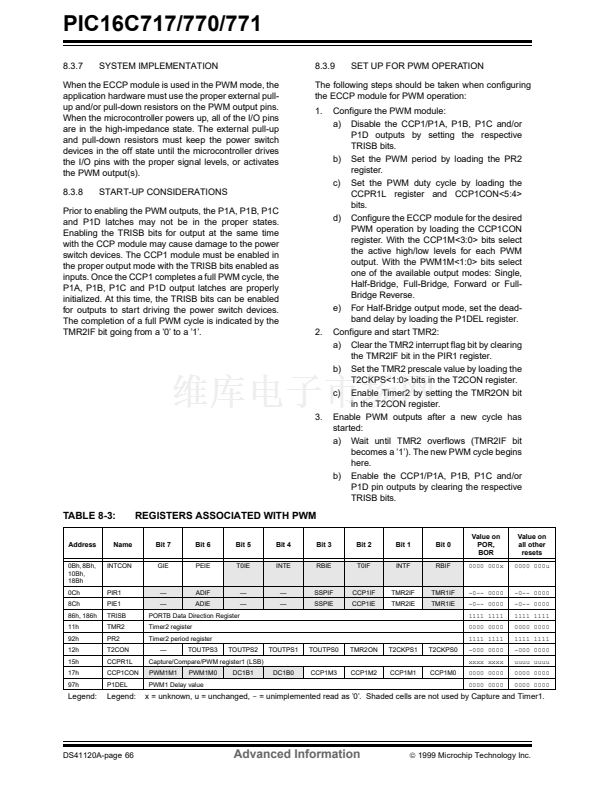
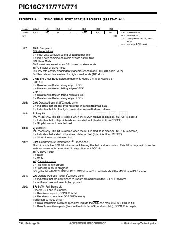
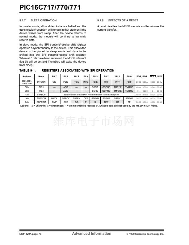
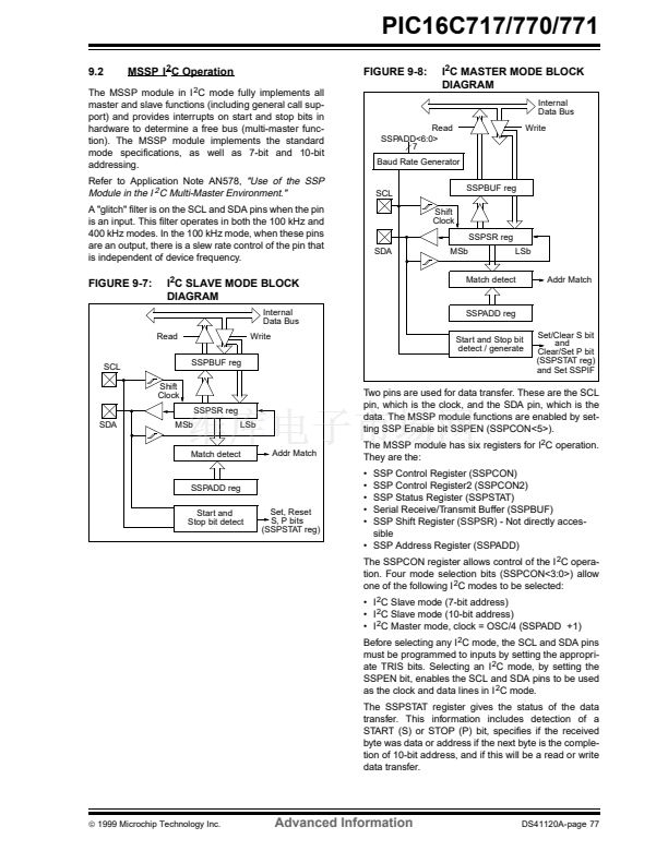
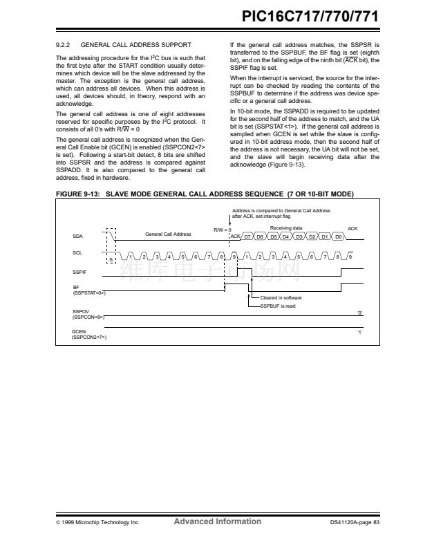
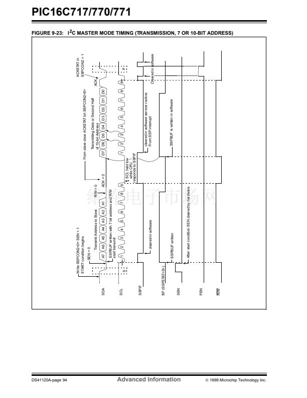
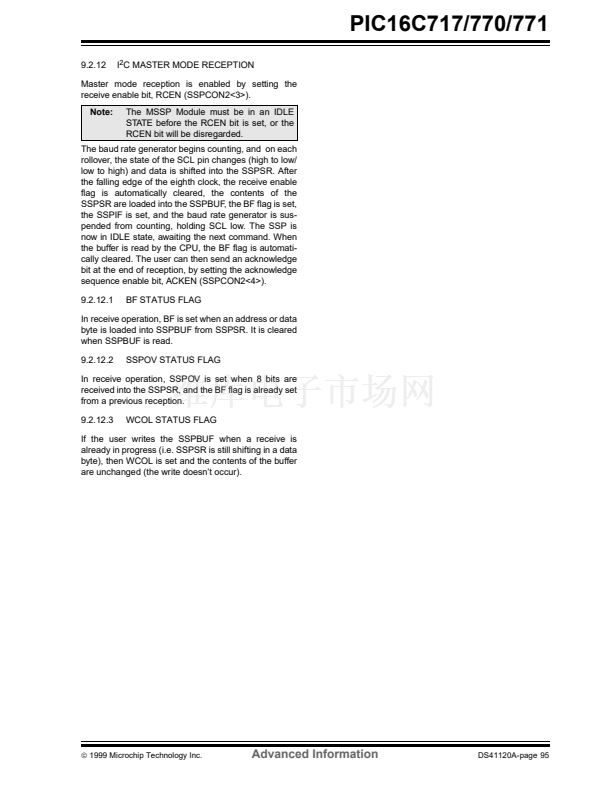
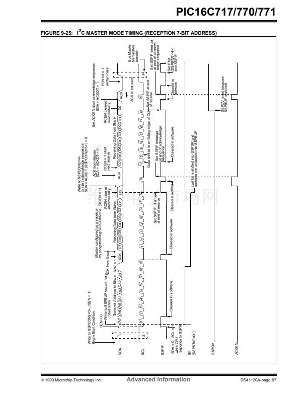
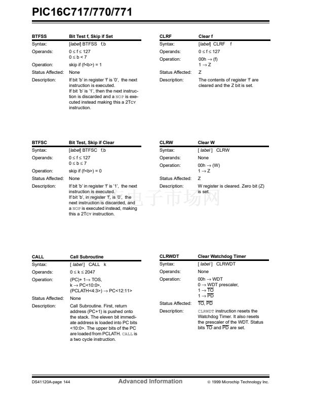
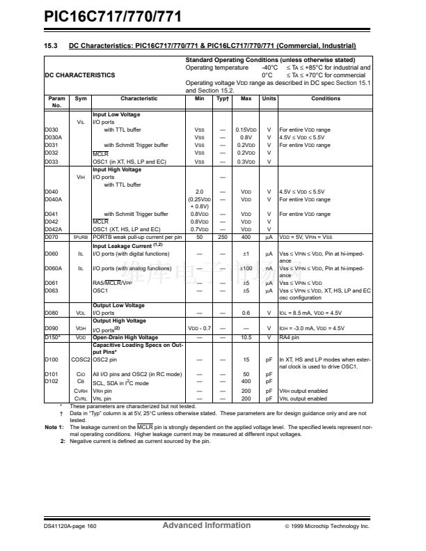
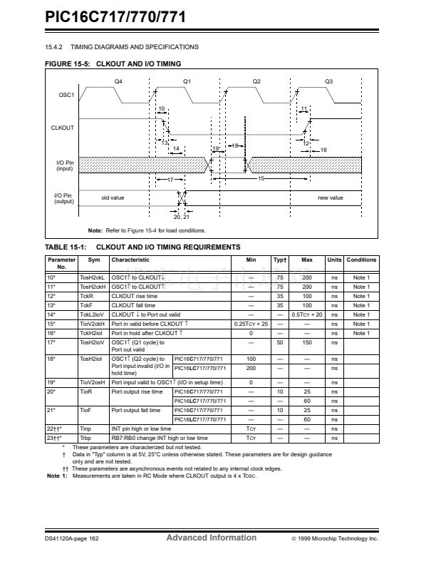
PIC16C717/770/771
1.0
DEVICE OVERVIEW
This document contains device-specific information.
Additional information may be found in the PICmicro
TM
Mid-Range Reference Manual, (DS33023), which may
be obtained from your local Microchip Sales Represen-
tative or downloaded from the Microchip website. The
Reference Manual should be considered a comple-
mentary document to this data sheet, and is highly rec-
ommended reading for a better understanding of the
device architecture and operation of the peripheral
modules.
There are three devices (PIC16C717, PIC16C770 and
PIC16C771) covered by this datasheet. The
PIC16C717 device comes in 18/20-pin packages and
the PIC16C770/771 devices come in 20-pin packages.
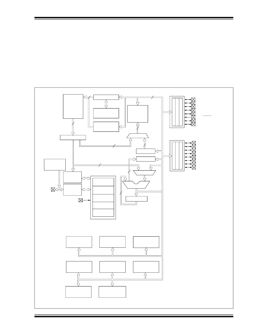
The following two figures are device block diagrams of
the PIC16C717 and the PIC16C770/771.
FIGURE 1-1:
PIC16C717 BLOCK DIAGRAM
13
EPROM
Program
Memory
2K x 14
8 Level Stack
(13-bit)
Program Memory
Read (PMR)
Program Counter
Data Bus
8
PORTA
RA0/AN0
RA1/AN1/LVDIN
RA2/AN2/V
REF
-/VRL
RA3/AN3/V
REF
+/VRH
RA4/T0CKI
RA5/MCLR/V
PP
RA6/OSC2/CLKOUT
RA7/OSC1/CLKIN
RAM
File
Registers
256 x 8
9
Addr MUX
RAM
Addr
(1)
Program
Bus
14
Instruction reg
Direct Addr
7
PORTB
Indirect
Addr
RB0/AN4/INT
RB1/AN5/SS
RB2/SCK/SCL
RB3/CCP1/P1A
RB4/SDI/SDA
RB5/SDO/P1B
RB6/T1OSO/T1CKI/P1C
RB7/T1OSI/P1O
8
FSR reg
Internal
4MHz, 37KHz
and ER mode
Instruction
Decode &
Control
Timing
Generation
V
DD
, V
SS
8
STATUS reg
3
Power-up
Timer
Oscillator
Start-up Timer
Power-on
Reset
Watchdog
Timer
Brown-out
Reset
ALU
8
W reg
MUX
OSC1/CLKIN
OSC2/CLKOUT
10-bit
ADC
Bandgap
Reference
Low-voltage
Detect
Timer0
Timer1
Timer2
Enhanced CCP
(ECCP1)
Master
Synchronous
Serial Port (MSSP)
Note 1:
Higher order bits are from the STATUS register.
漏
1999 Microchip Technology Inc.
Advanced Information
DS41120A-page 5


 1
1
 2
2
 3
3
 4
4
 5
5
 6
6
 7
7
 8
8
 9
9
 10
10
 11
11
 12
12
 13
13
 14
14
 15
15
 16
16
 17
17
 18
18
 19
19
 20
20
 21
21
 22
22
 23
23
 24
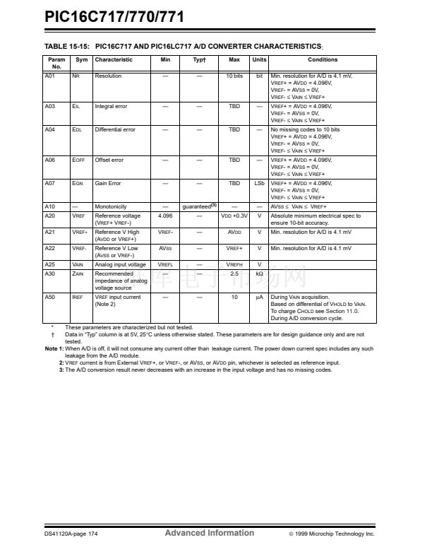
24
 25
25
 26
26
 27
27
 28
28
 29
29
 30
30
 31
31
 32
32
 33
33
 34
34
 35
35
 36
36
 37
37
 38
38
 39
39
 40
40
 41
41
 42
42
 43
43
 44
44
 45
45
 46
46
 47
47
 48
48
 49
49
 50
50
 51
51
 52
52
 53
53
 54
54
 55
55
 56
56
 57
57
 58
58
 59
59
 60
60
 61
61
 62
62
 63
63
 64
64
 65
65
 66
66
 67
67
 68
68
 69
69
 70
70
 71
71
 72
72
 73
73
 74
74
 75
75
 76
76
 77
77
 78
78
 79
79
 80
80
 81
81
 82
82
 83
83
 84
84
 85
85
 86
86
 87
87
 88
88
 89
89
 90
90
 91
91
 92
92
 93
93
 94
94
 95
95
 96
96
 97
97
 98
98
 99
99
 100
100
 101
101
 102
102
 103
103
 104
104
 105
105
 106
106
 107
107
 108
108
 109
109
 110
110
 111
111
 112
112
 113
113
 114
114
 115
115
 116
116
 117
117
 118
118
 119
119
 120
120
 121
121
 122
122
 123
123
 124
124
 125
125
 126
126
 127
127
 128
128
 129
129
 130
130
 131
131
 132
132
 133
133
 134
134
 135
135
 136
136
 137
137
 138
138
 139
139
 140
140
 141
141
 142
142
 143
143
 144
144
 145
145
 146
146
 147
147
 148
148
 149
149
 150
150
 151
151
 152
152
 153
153
 154
154
 155
155
 156
156
 157
157
 158
158
 159
159
 160
160
 161
161
 162
162
 163
163
 164
164
 165
165
 166
166
 167
167
 168
168
 169
169
 170
170
 171
171
 172
172
 173
173
 174
174
 175
175
 176
176
 177
177
 178
178
 179
179
 180
180
 181
181
 182
182
 183
183
 184
184
 185
185
 186
186
 187
187
 188
188
 189
189
 190
190
 191
191
 192
192
 193
193
 194
194
 195
195
 196
196
 197
197
 198
198
 199
199
 200
200
