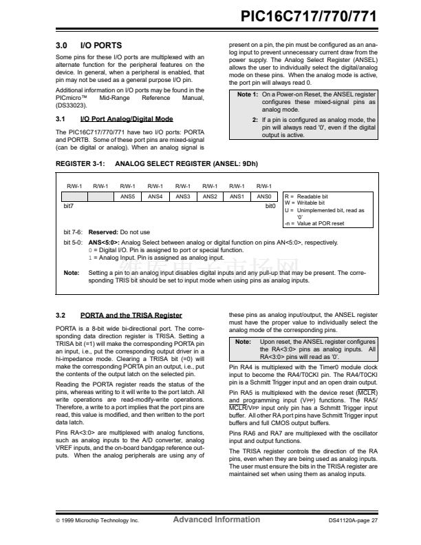
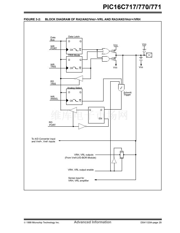
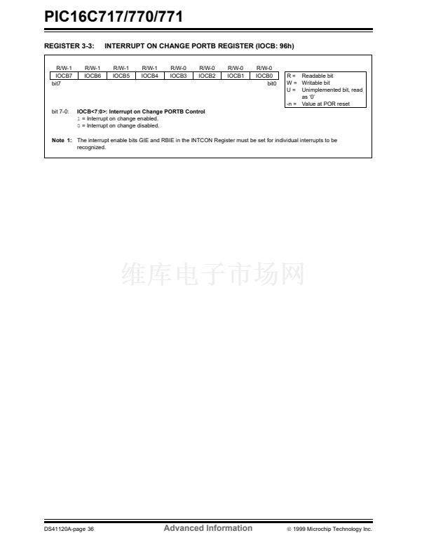
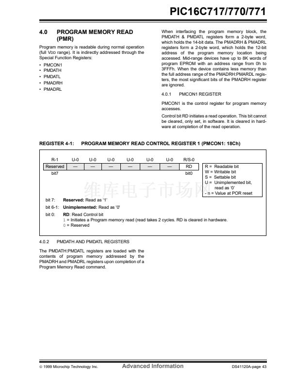
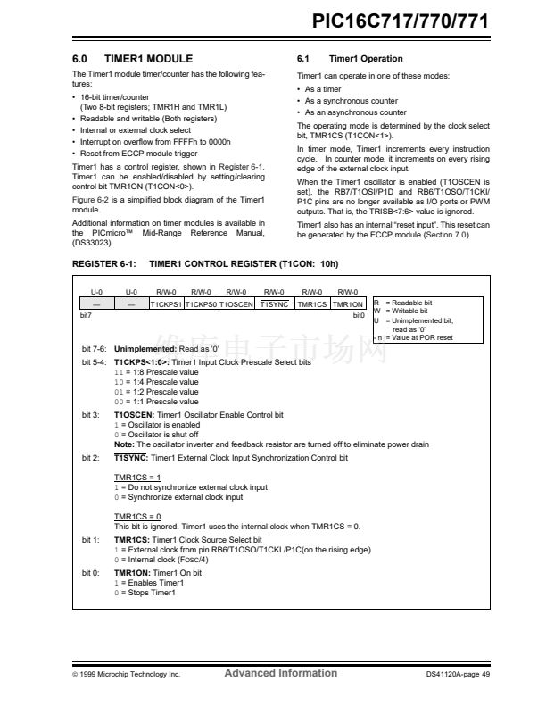
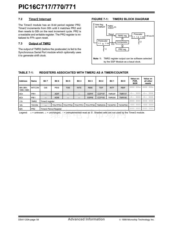
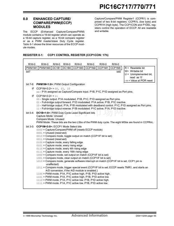
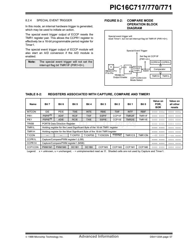
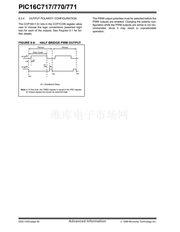
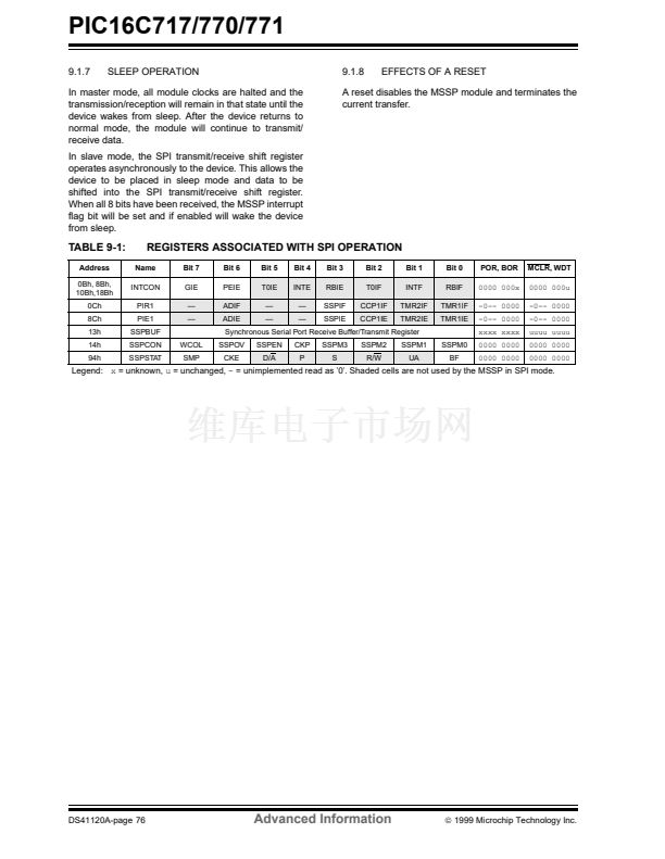
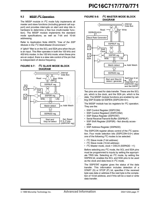
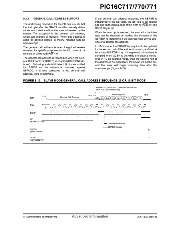
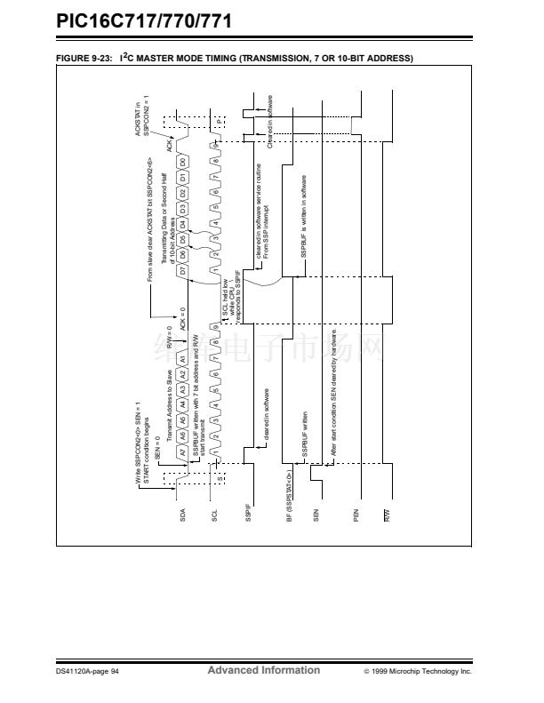
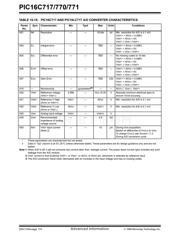
PIC16C717/770/771
8.3.5
PROGRAMMABLE DEADBAND DELAY
In half-bridge or full-bridge applications, where all
power switches are modulated at the PWM frequency
at all time, the power switches normally require longer
time to turn off than to turn on. If both the upper and
lower power switches are switched at the same time
(one turned on, and the other turned off), both switches
will be on for a short period of time, until one switch
completely turns off. During this time, a very high cur-
rent, called shoot-through current, will flow through
both power switches, shorting the bridge supply. To
avoid this potentially destructive shoot-through current
from flowing during switching, turning on the power
switch is normally delayed to allow the other switch to
completely turn off.
In the Half-Bridge Output mode, a digitally program-
mable deadband delay is available to avoid shoot-
through current from destroying the bridge power
switches. The delay occurs at the signal transition from
the non-active state to the active state. See
Figure 8-6
for illustration. The P1DEL register sets the amount of
delay.
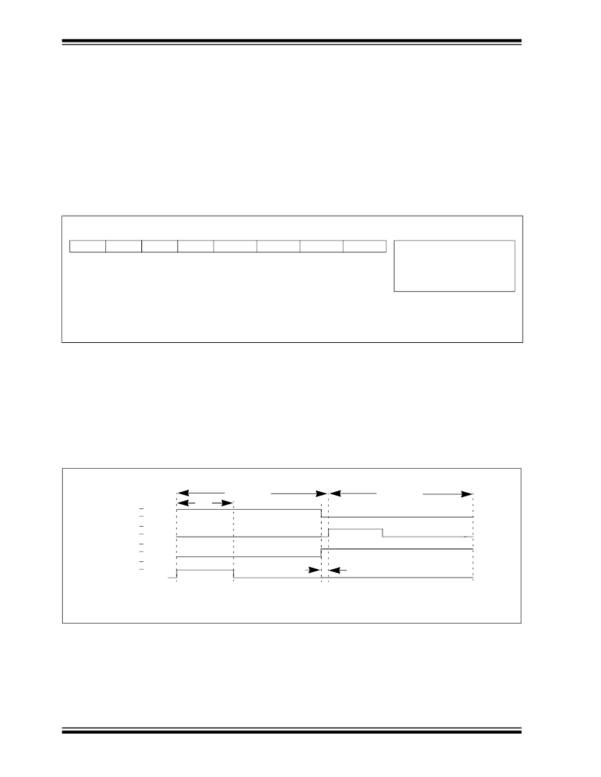
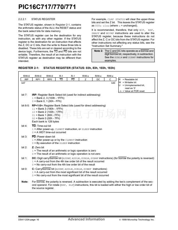
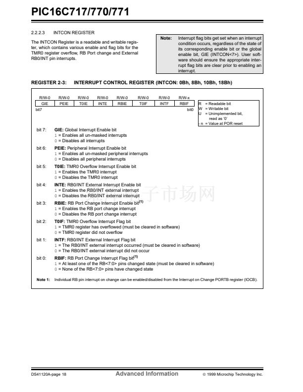
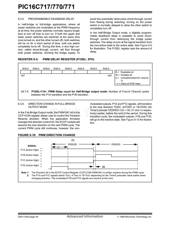
REGISTER 8-2:
R/W-0
bit7
R/W-0
PWM DELAY REGISTER (P1DEL: 97H)
R/W-0
R/W-0
R/W-0
R/W-0
R/W-0
R/W-0
bit0
R = Readable bit
W = Writable bit
U = Unimplemented bit, read as
鈥?鈥?/div>
- n = Value at POR reset
bit 7-0:
P1DEL<7:0>: PWM Delay count for Half-Bridge output mode:
Number of F
OSC
/4 (Tosc
鈥?/div>
4) cycles
between the P1A transition and the P1B transition.
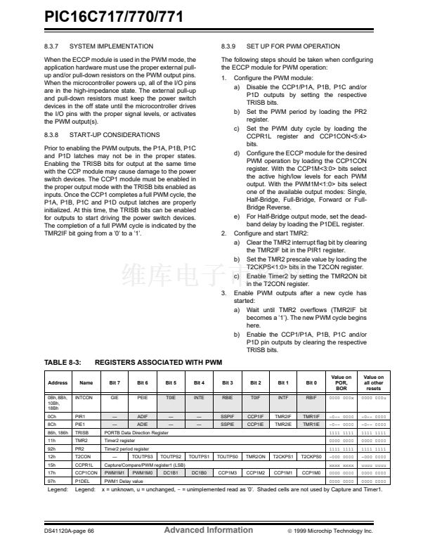
8.3.6
DIRECTION CHANGE IN FULL-BRIDGE
OUTPUT MODE
In the Full-Bridge Output mode, the PWM1M1 bit in the
CCP1CON register allows user to control the Forward/
Reverse direction. When the application firmware
changes this direction control bit, the ECCP module will
assume the new direction on the next PWM cycle. The
current PWM cycle still continues, however, the non-
modulated outputs, P1A and P1C signals, will transition
to the new direction TOSC, 4
鈥?/div>
TOSC or 16
鈥?/div>
TOSC (for
Timer2 presale T2CKRS<1:0> = 00, 01 and 1x respec-
tively) earlier, before the end of the period. During this
transition cycle, the modulated outputs, P1B and P1D,
will go to the inactive state. See
Figure 8-10
for illustra-
tion.
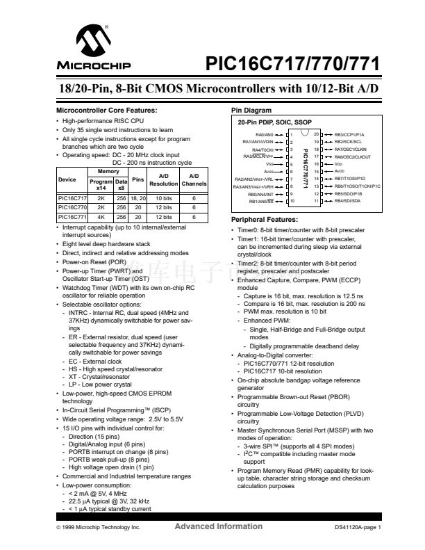
FIGURE 8-10: PWM DIRECTION CHANGE
(1)
SIGNAL
P1A (Active High)
P1B (Active High)
P1C (Active High)
P1D (Active High)
Note 1:
2:
(2)
PERIOD
DC
PERIOD
The Direction bit in the ECCP Control Register (CCP1CON.PWM1M1) is written anytime during the PWM cycle.
The P1A and P1C signals switch T
OSC
, 4*Tosc or 16*T
OSC
depending on the Timer2 prescaler value earlier when
changing direction. The modulated P1B and P1D signals are inactive at this time.
DS41120A-page 64
Advanced Information
漏
1999 Microchip Technology Inc.


 1
1
 2
2
 3
3
 4
4
 5
5
 6
6
 7
7
 8
8
 9
9
 10
10
 11
11
 12
12
 13
13
 14
14
 15
15
 16
16
 17
17
 18
18
 19
19
 20
20
 21
21
 22
22
 23
23
 24
24
 25
25
 26
26
 27
27
 28
28
 29
29
 30
30
 31
31
 32
32
 33
33
 34
34
 35
35
 36
36
 37
37
 38
38
 39
39
 40
40
 41
41
 42
42
 43
43
 44
44
 45
45
 46
46
 47
47
 48
48
 49
49
 50
50
 51
51
 52
52
 53
53
 54
54
 55
55
 56
56
 57
57
 58
58
 59
59
 60
60
 61
61
 62
62
 63
63
 64
64
 65
65
 66
66
 67
67
 68
68
 69
69
 70
70
 71
71
 72
72
 73
73
 74
74
 75
75
 76
76
 77
77
 78
78
 79
79
 80
80
 81
81
 82
82
 83
83
 84
84
 85
85
 86
86
 87
87
 88
88
 89
89
 90
90
 91
91
 92
92
 93
93
 94
94
 95
95
 96
96
 97
97
 98
98
 99
99
 100
100
 101
101
 102
102
 103
103
 104
104
 105
105
 106
106
 107
107
 108
108
 109
109
 110
110
 111
111
 112
112
 113
113
 114
114
 115
115
 116
116
 117
117
 118
118
 119
119
 120
120
 121
121
 122
122
 123
123
 124
124
 125
125
 126
126
 127
127
 128
128
 129
129
 130
130
 131
131
 132
132
 133
133
 134
134
 135
135
 136
136
 137
137
 138
138
 139
139
 140
140
 141
141
 142
142
 143
143
 144
144
 145
145
 146
146
 147
147
 148
148
 149
149
 150
150
 151
151
 152
152
 153
153
 154
154
 155
155
 156
156
 157
157
 158
158
 159
159
 160
160
 161
161
 162
162
 163
163
 164
164
 165
165
 166
166
 167
167
 168
168
 169
169
 170
170
 171
171
 172
172
 173
173
 174
174
 175
175
 176
176
 177
177
 178
178
 179
179
 180
180
 181
181
 182
182
 183
183
 184
184
 185
185
 186
186
 187
187
 188
188
 189
189
 190
190
 191
191
 192
192
 193
193
 194
194
 195
195
 196
196
 197
197
 198
198
 199
199
 200
200
