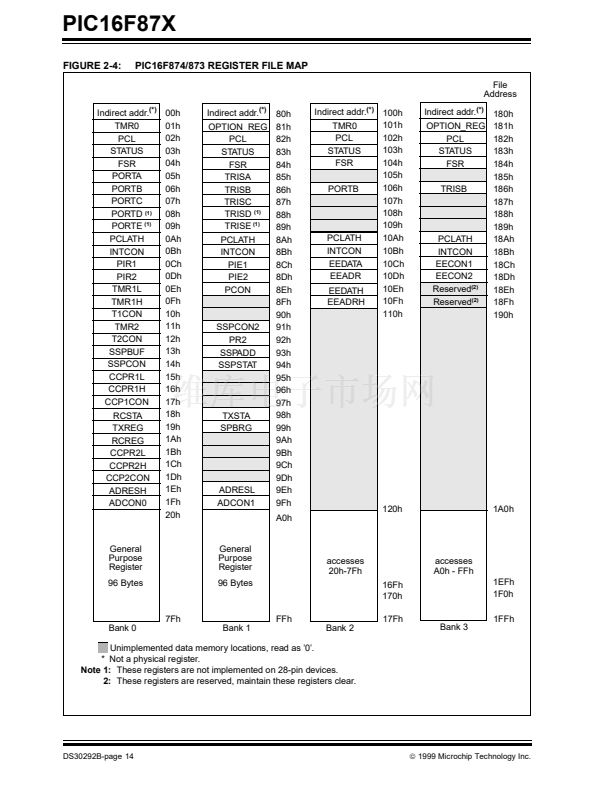
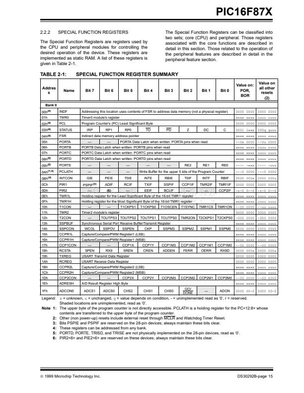
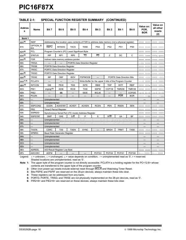
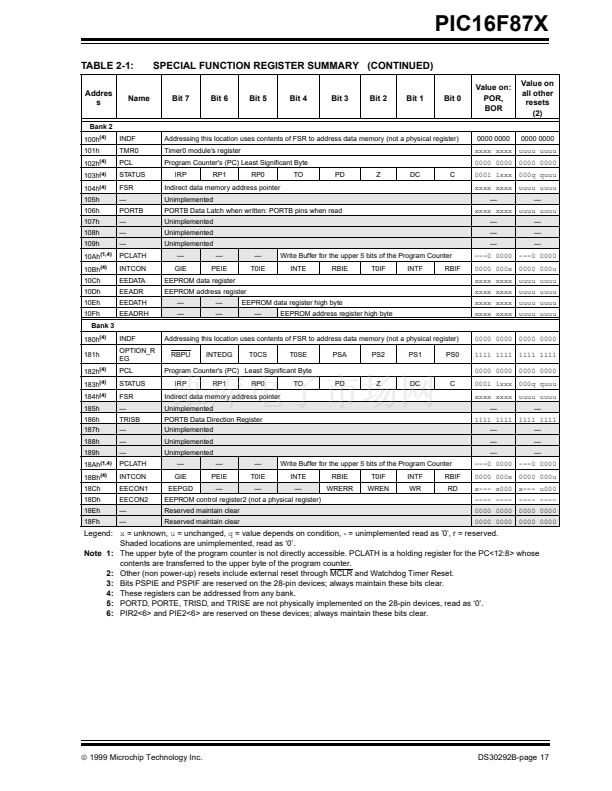
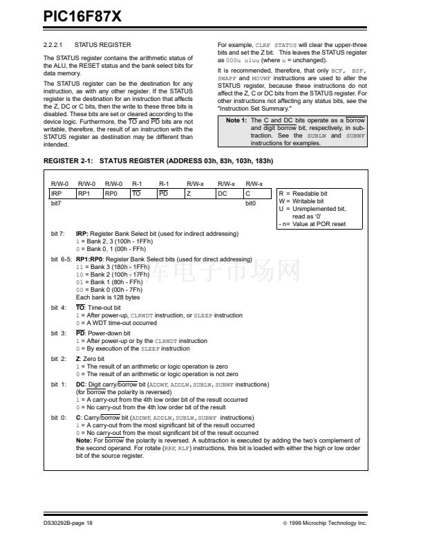
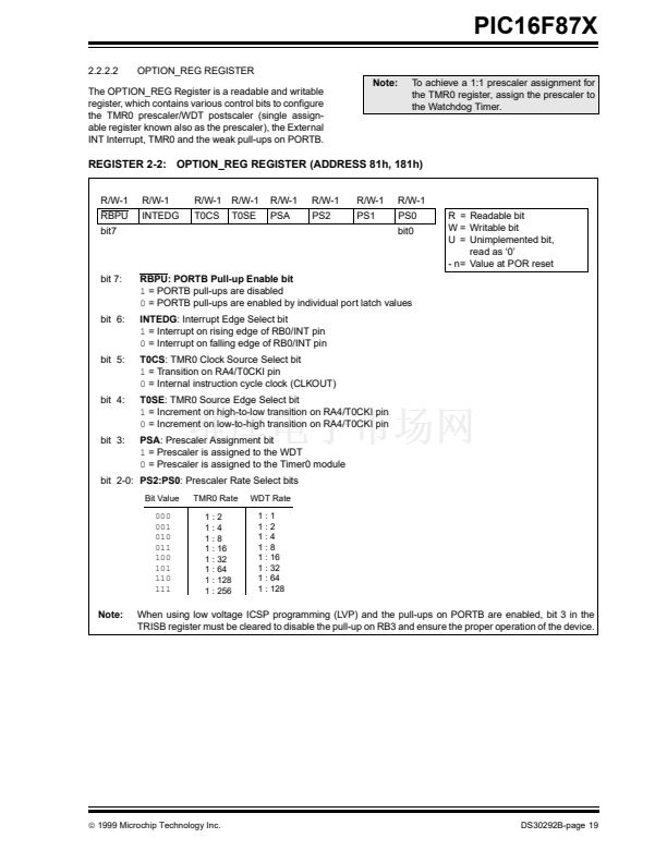
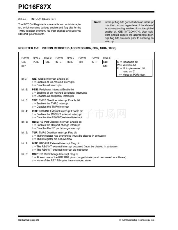
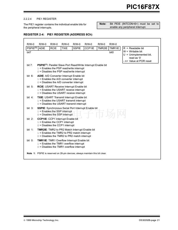
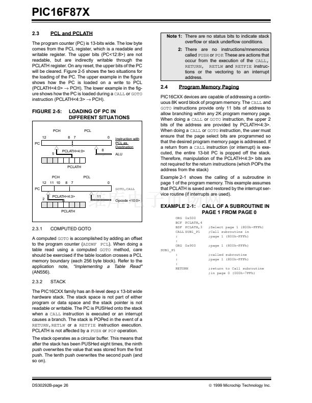
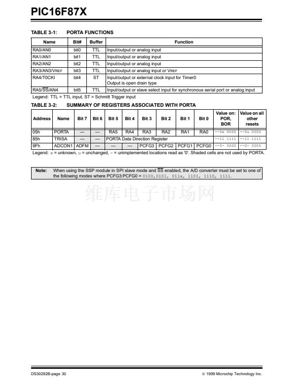
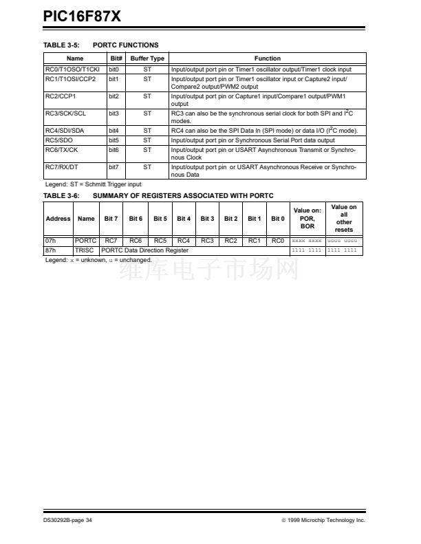
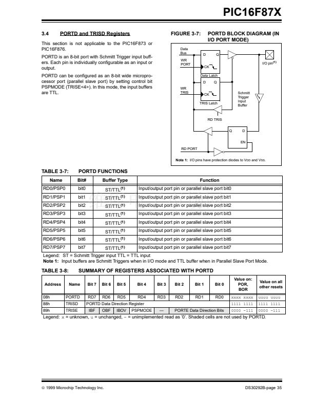
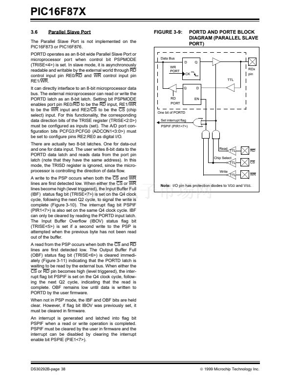
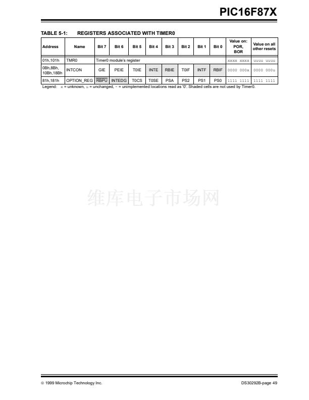
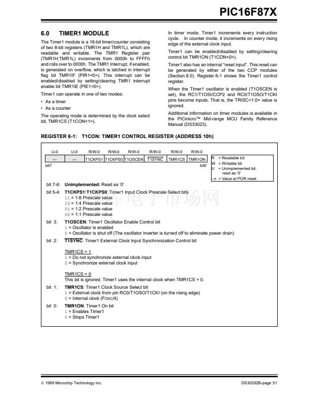
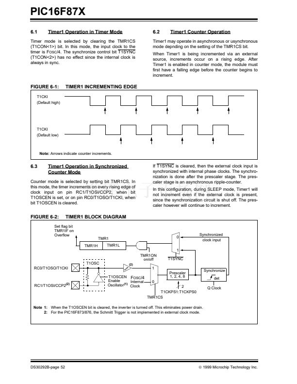
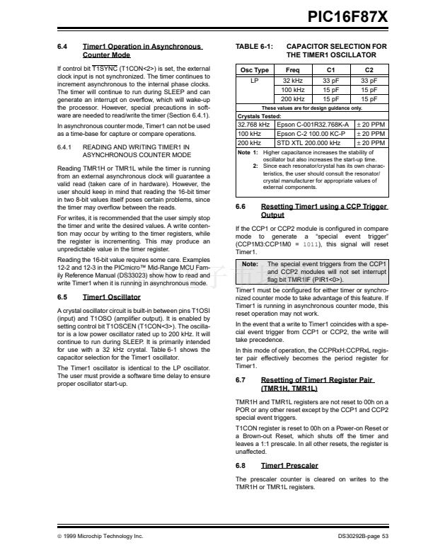
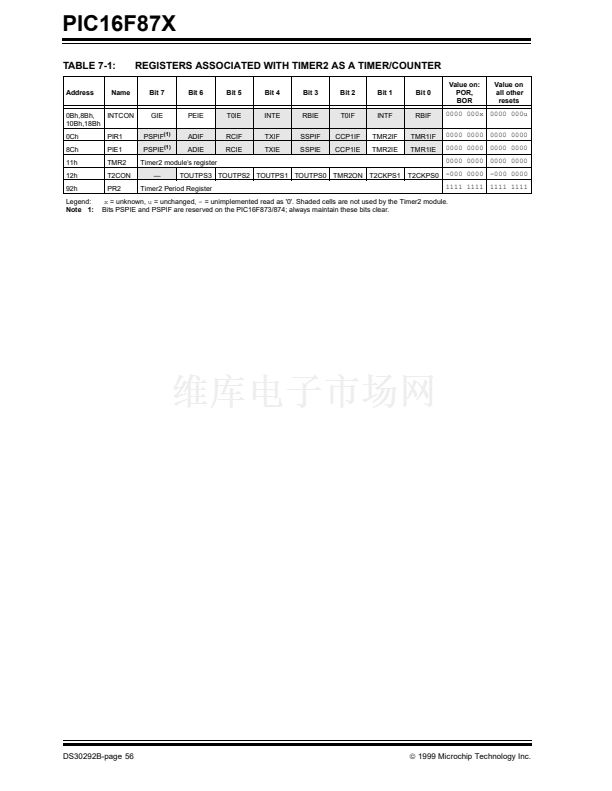
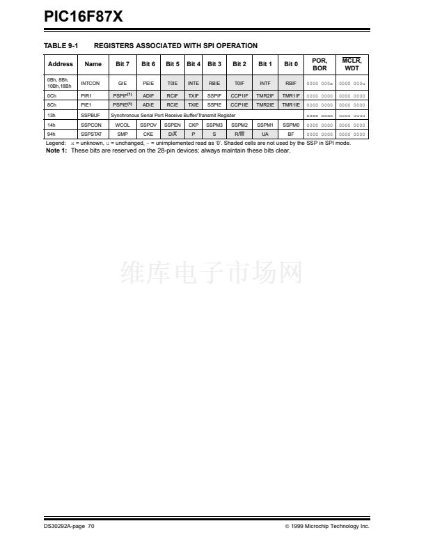
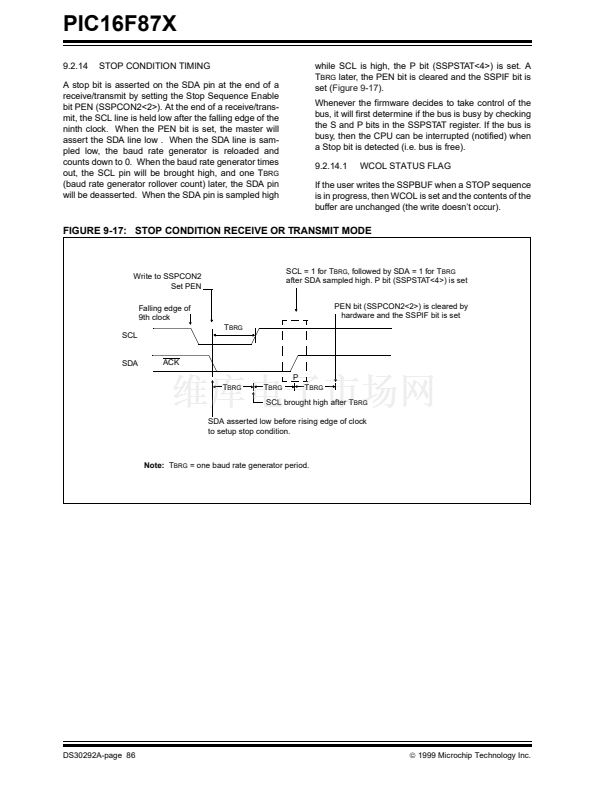
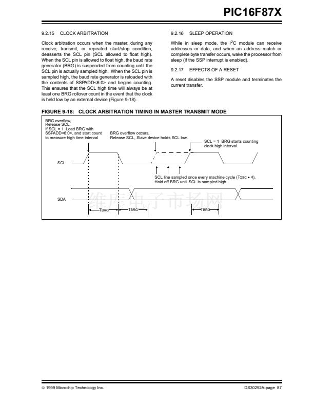
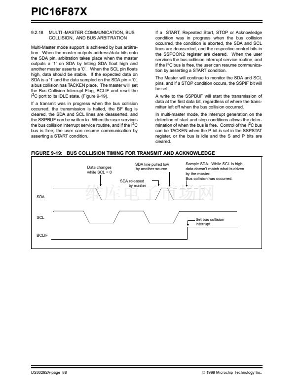
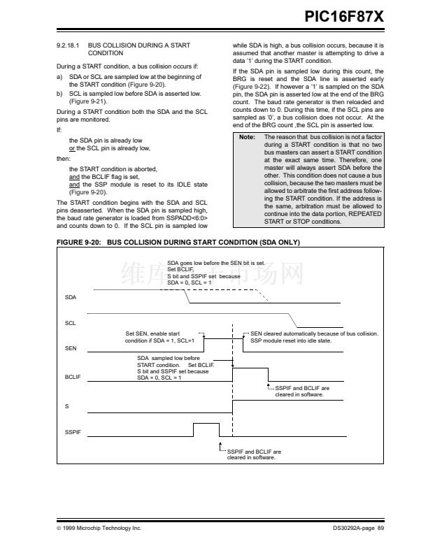
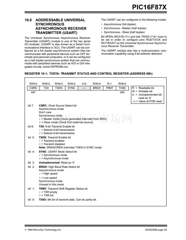
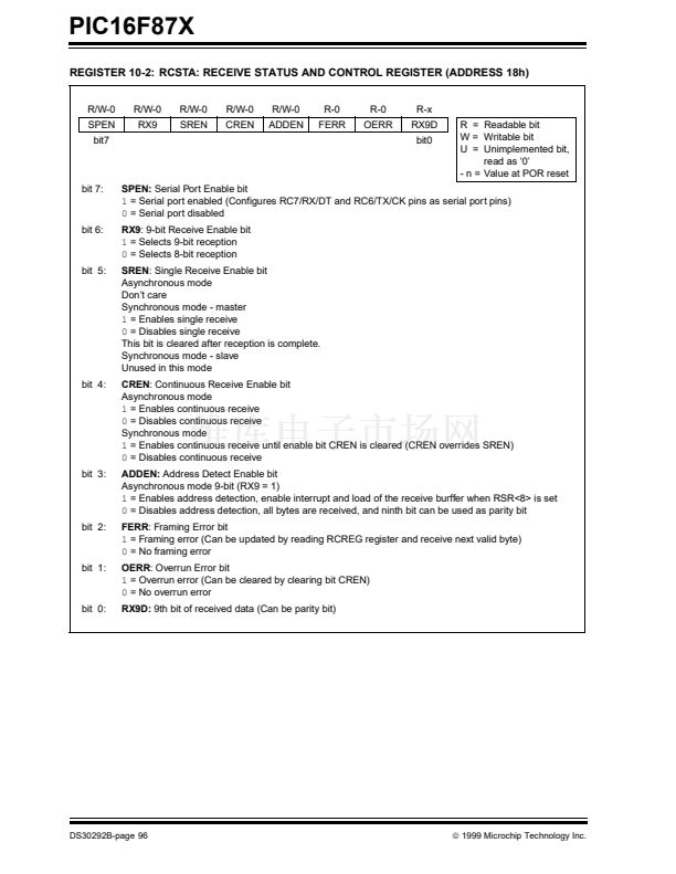
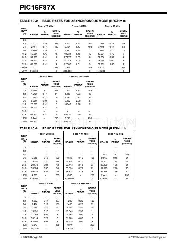
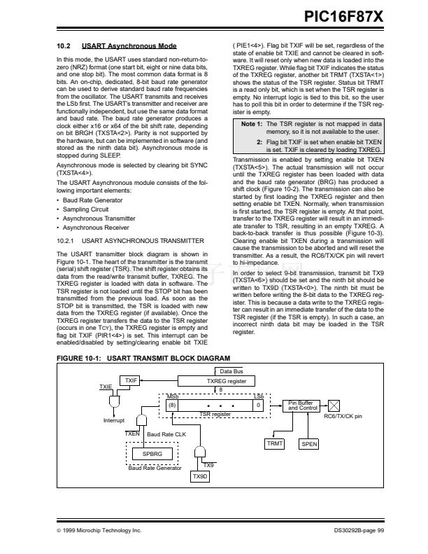
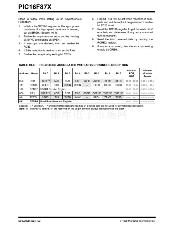
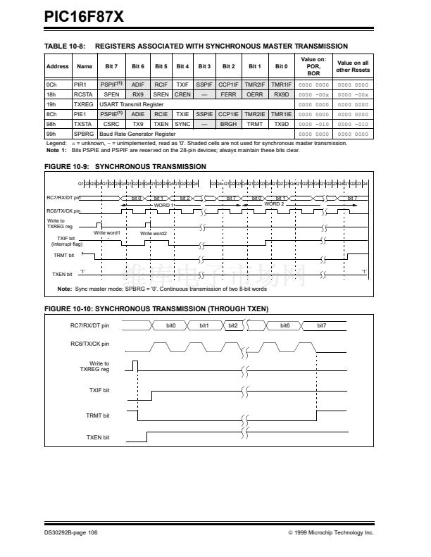
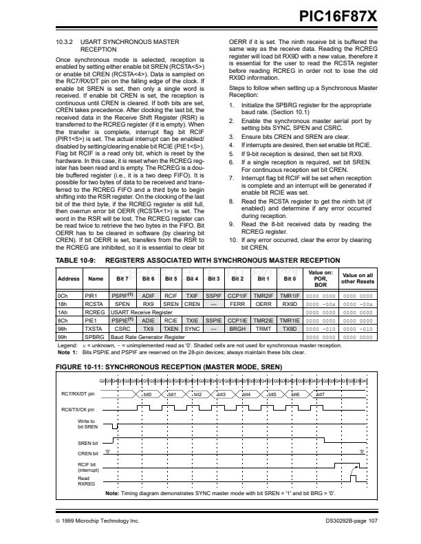
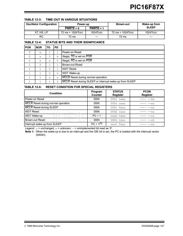
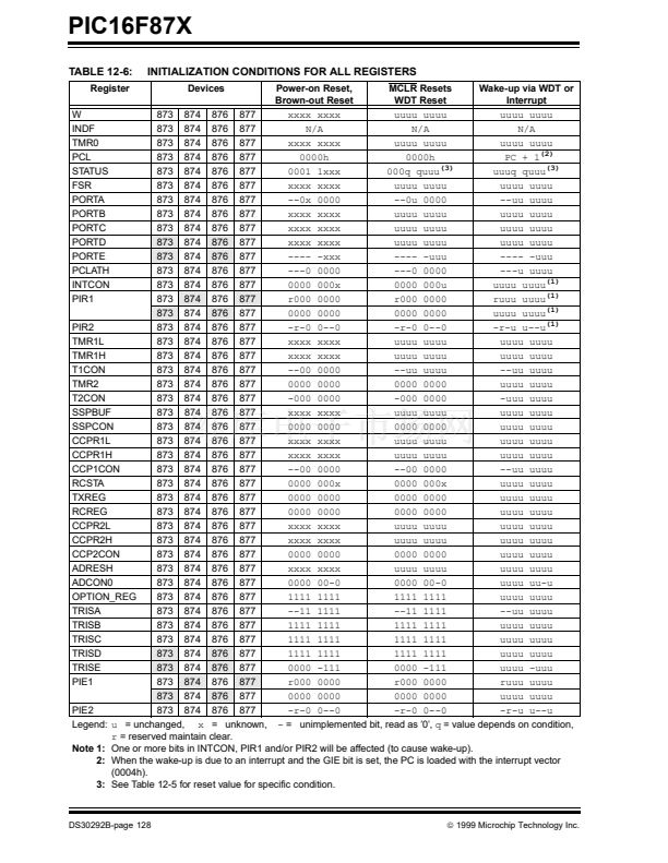
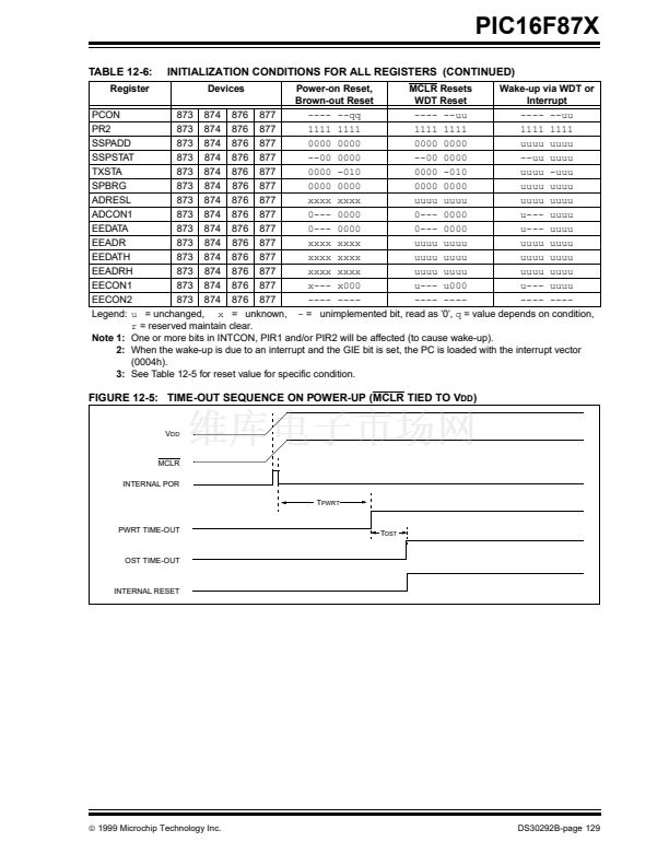
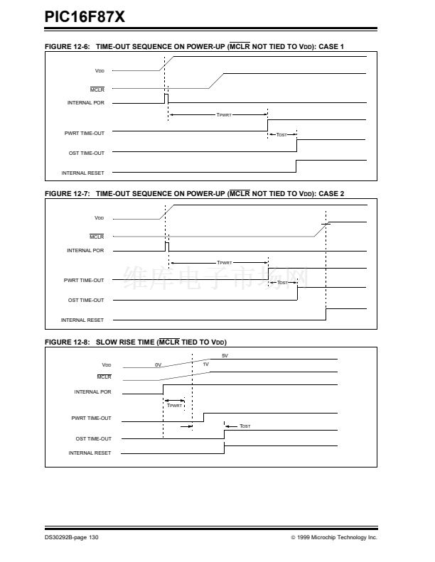
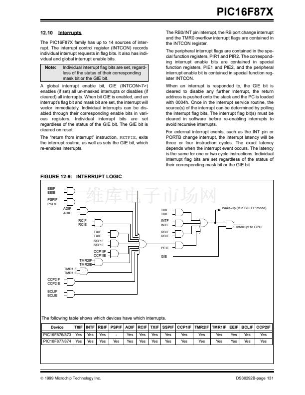
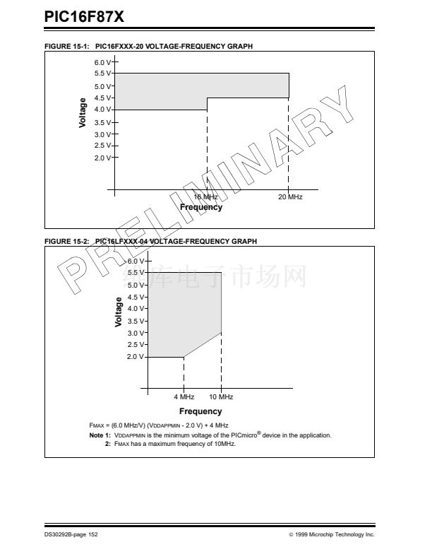
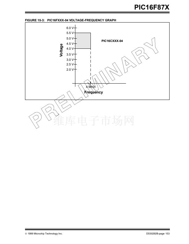
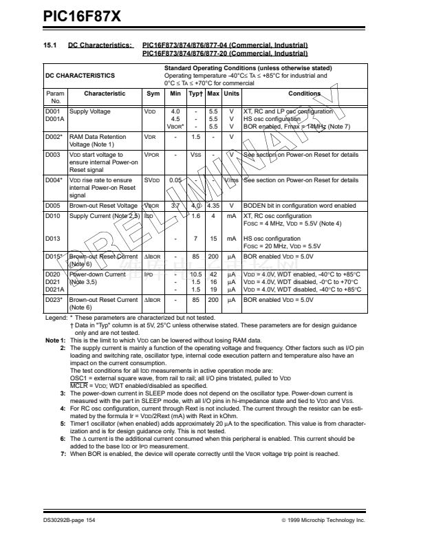
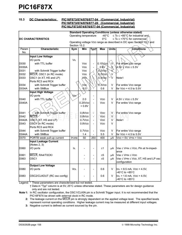
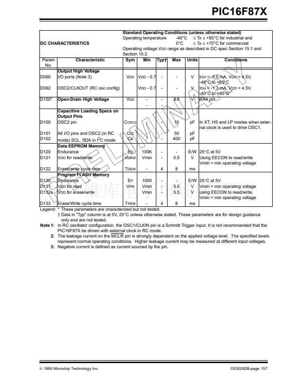
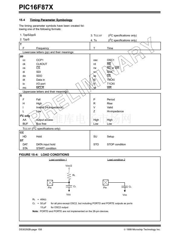
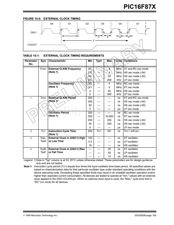
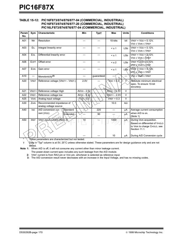
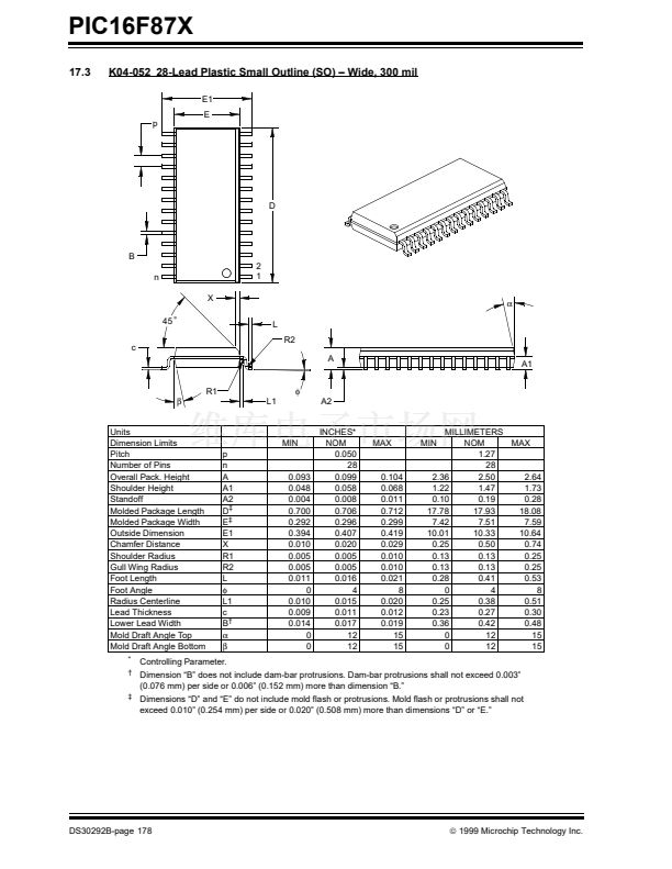
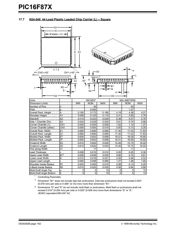
PIC16F87X
3.5
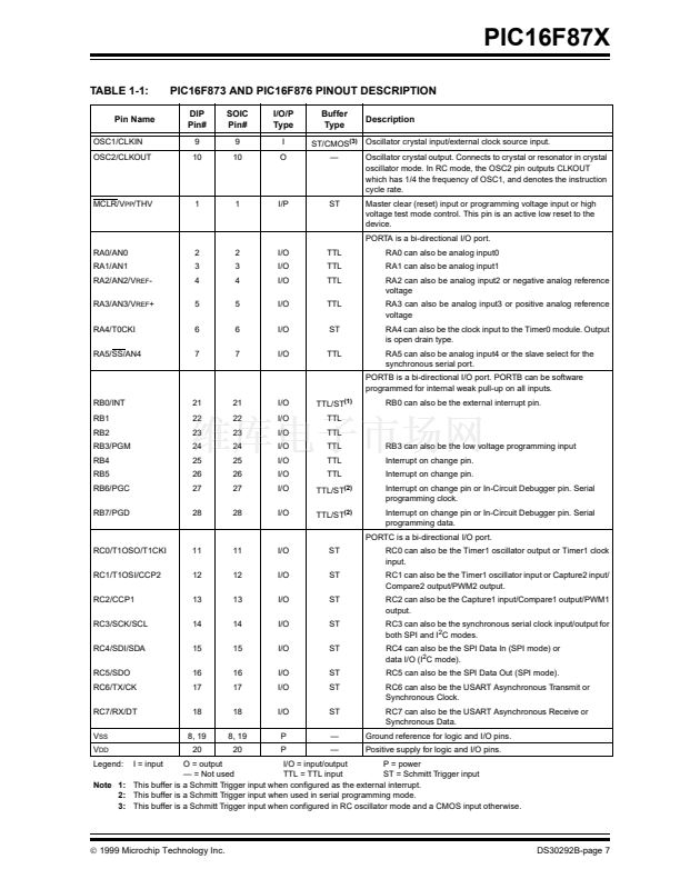
PORTE and TRISE Register
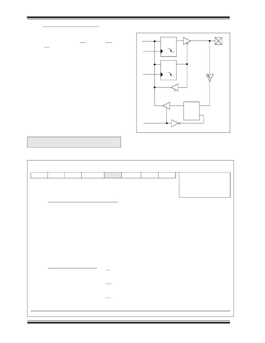
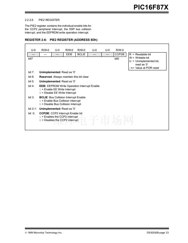
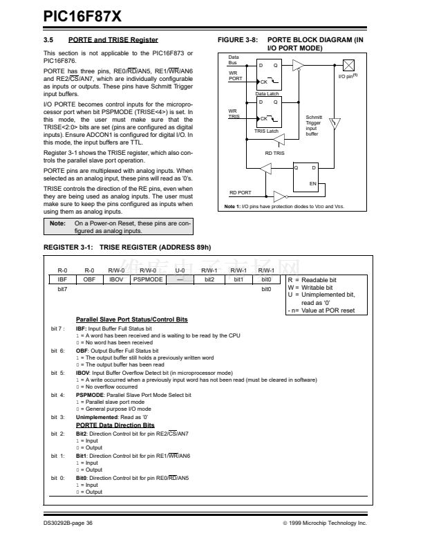
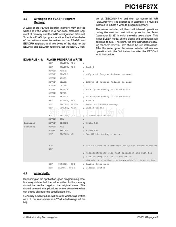
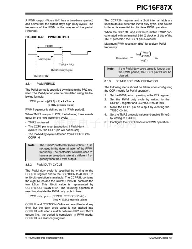
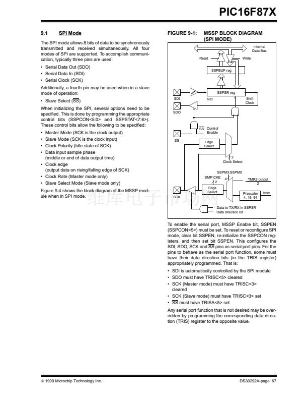
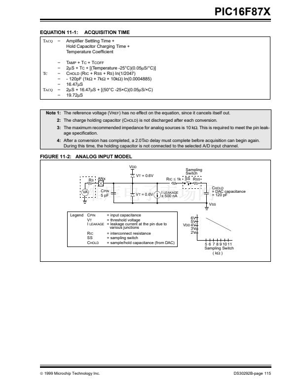
FIGURE 3-8:
Data
Bus
WR
PORT
This section is not applicable to the PIC16F873 or
PIC16F876.
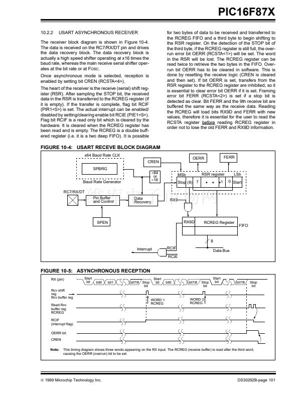
PORTE has three pins, RE0/RD/AN5, RE1/WR/AN6
and RE2/CS/AN7, which are individually configurable
as inputs or outputs. These pins have Schmitt Trigger
input buffers.
I/O PORTE becomes control inputs for the micropro-
cessor port when bit PSPMODE (TRISE<4>) is set. In
this mode, the user must make sure that the
TRISE<2:0> bits are set (pins are configured as digital
inputs). Ensure ADCON1 is configured for digital I/O. In
this mode, the input buffers are TTL.
Register 3-1 shows the TRISE register, which also con-
trols the parallel slave port operation.
PORTE pins are multiplexed with analog inputs. When
selected as an analog input, these pins will read as 鈥?鈥檚.
TRISE controls the direction of the RE pins, even when
they are being used as analog inputs. The user must
make sure to keep the pins configured as inputs when
using them as analog inputs.
Note:
On a Power-on Reset, these pins are con-
figured as analog inputs.
PORTE BLOCK DIAGRAM (IN
I/O PORT MODE)
D
Q
I/O pin
(1)
CK
Data Latch
D
WR
TRIS
Q
Schmitt
Trigger
input
buffer
CK
TRIS Latch
RD TRIS
Q
D
EN
EN
RD PORT
Note 1:
I/O pins have protection diodes to V
DD
and V
SS
.
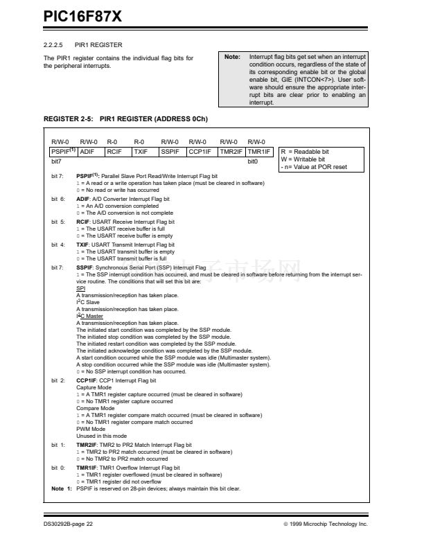
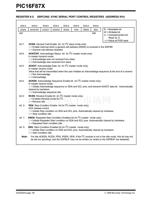
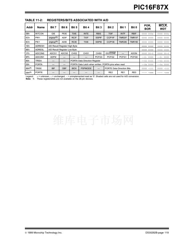
REGISTER 3-1: TRISE REGISTER (ADDRESS 89h)
R-0
IBF
bit7
R-0
OBF
R/W-0
IBOV
R/W-0
PSPMODE
U-0
鈥?/div>
R/W-1
bit2
R/W-1
bit1
R/W-1
bit0
bit0
R = Readable bit
W = Writable bit
U = Unimplemented bit,
read as 鈥?鈥?/div>
- n= Value at POR reset
Parallel Slave Port Status/Control Bits
bit 7 :
IBF:
Input Buffer Full Status bit
1
= A word has been received and is waiting to be read by the CPU
0
= No word has been received
OBF:
Output Buffer Full Status bit
1
= The output buffer still holds a previously written word
0
= The output buffer has been read
IBOV:
Input Buffer Overflow Detect bit (in microprocessor mode)
1
= A write occurred when a previously input word has not been read (must be cleared in software)
0
= No overflow occurred
PSPMODE:
Parallel Slave Port Mode Select bit
1
= Parallel slave port mode
0
= General purpose I/O mode
Unimplemented:
Read as 鈥?鈥?/div>
bit 6:
bit 5:
bit 4:
bit 3:
bit 2:
PORTE Data Direction Bits
Bit2:
Direction Control bit for pin RE2/CS/AN7
1
= Input
0
= Output
Bit1:
Direction Control bit for pin RE1/WR/AN6
1
= Input
0
= Output
Bit0:
Direction Control bit for pin RE0/RD/AN5
1
= Input
0
= Output
bit 1:
bit 0:
DS30292B-page 36
漏
1999 Microchip Technology Inc.


 1
1
 2
2
 3
3
 4
4
 5
5
 6
6
 7
7
 8
8
 9
9
 10
10
 11
11
 12
12
 13
13
 14
14
 15
15
 16
16
 17
17
 18
18
 19
19
 20
20
 21
21
 22
22
 23
23
 24
24
 25
25
 26
26
 27
27
 28
28
 29
29
 30
30
 31
31
 32
32
 33
33
 34
34
 35
35
 36
36
 37
37
 38
38
 39
39
 40
40
 41
41
 42
42
 43
43
 44
44
 45
45
 46
46
 47
47
 48
48
 49
49
 50
50
 51
51
 52
52
 53
53
 54
54
 55
55
 56
56
 57
57
 58
58
 59
59
 60
60
 61
61
 62
62
 63
63
 64
64
 65
65
 66
66
 67
67
 68
68
 69
69
 70
70
 71
71
 72
72
 73
73
 74
74
 75
75
 76
76
 77
77
 78
78
 79
79
 80
80
 81
81
 82
82
 83
83
 84
84
 85
85
 86
86
 87
87
 88
88
 89
89
 90
90
 91
91
 92
92
 93
93
 94
94
 95
95
 96
96
 97
97
 98
98
 99
99
 100
100
 101
101
 102
102
 103
103
 104
104
 105
105
 106
106
 107
107
 108
108
 109
109
 110
110
 111
111
 112
112
 113
113
 114
114
 115
115
 116
116
 117
117
 118
118
 119
119
 120
120
 121
121
 122
122
 123
123
 124
124
 125
125
 126
126
 127
127
 128
128
 129
129
 130
130
 131
131
 132
132
 133
133
 134
134
 135
135
 136
136
 137
137
 138
138
 139
139
 140
140
 141
141
 142
142
 143
143
 144
144
 145
145
 146
146
 147
147
 148
148
 149
149
 150
150
 151
151
 152
152
 153
153
 154
154
 155
155
 156
156
 157
157
 158
158
 159
159
 160
160
 161
161
 162
162
 163
163
 164
164
 165
165
 166
166
 167
167
 168
168
 169
169
 170
170
 171
171
 172
172
 173
173
 174
174
 175
175
 176
176
 177
177
 178
178
 179
179
 180
180
 181
181
 182
182
 183
183
 184
184
 185
185
 186
186
 187
187
 188
188
 189
189
 190
190
 191
191
 192
192
 193
193
 194
194
 195
195
 196
196
 197
197
 198
198
 199
199
 200
200
