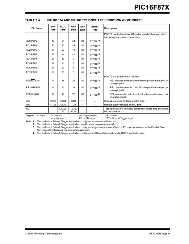
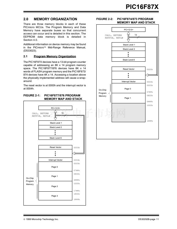
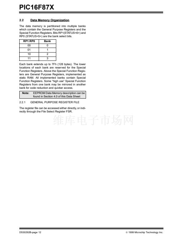
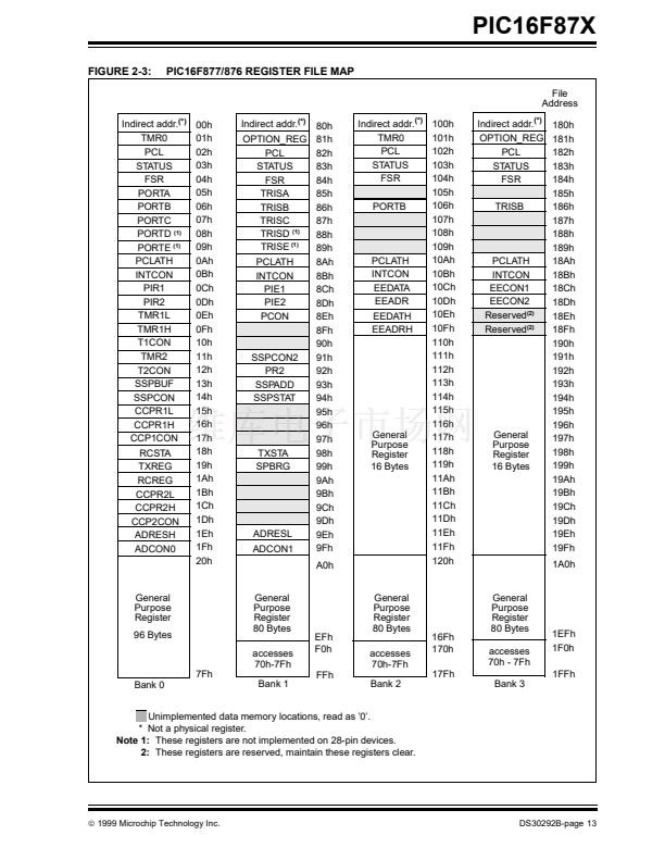
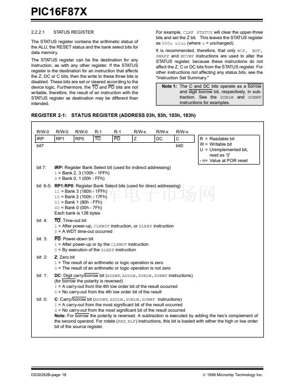
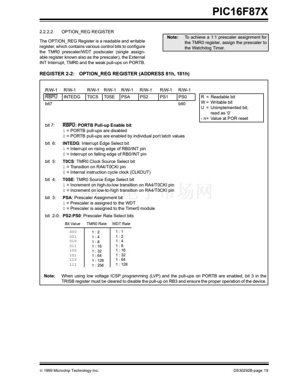
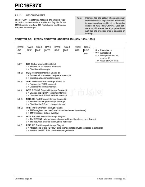
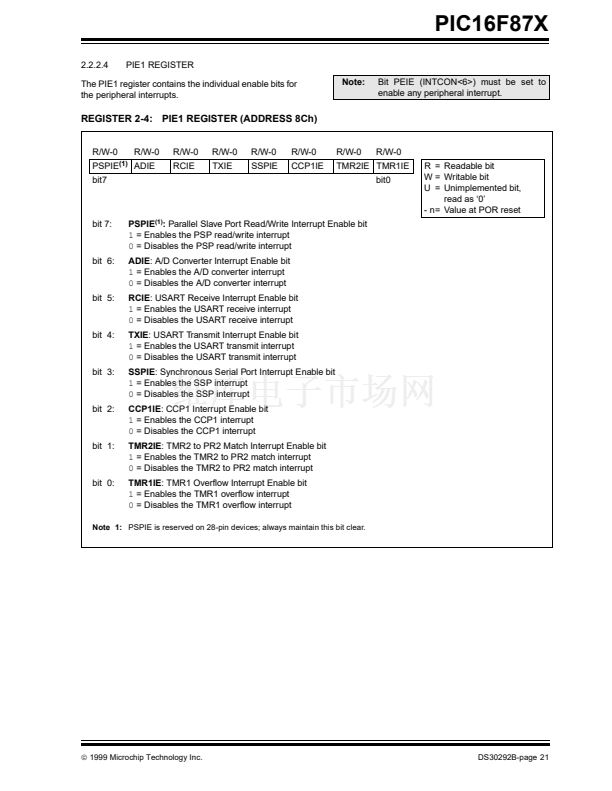
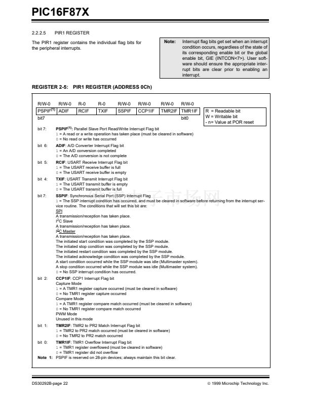
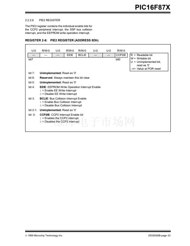
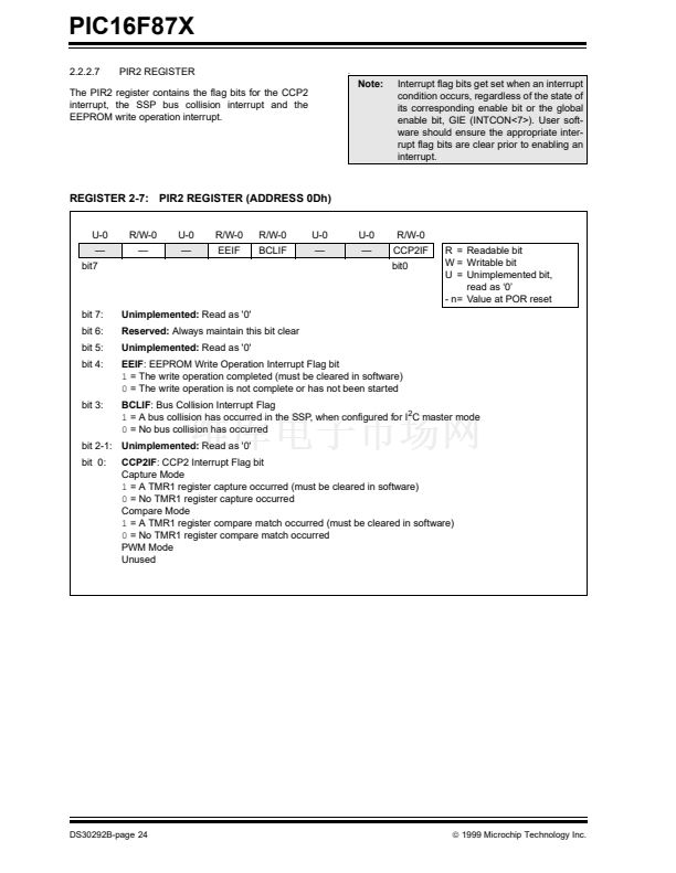
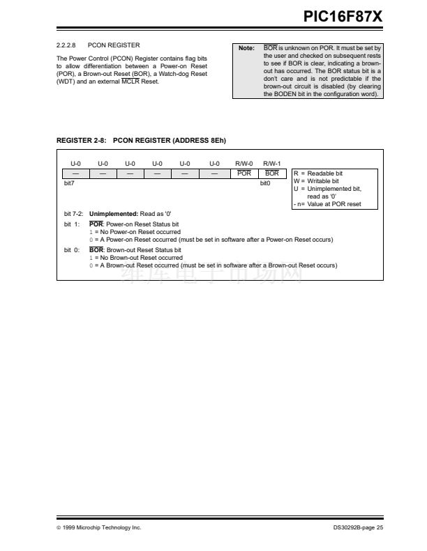
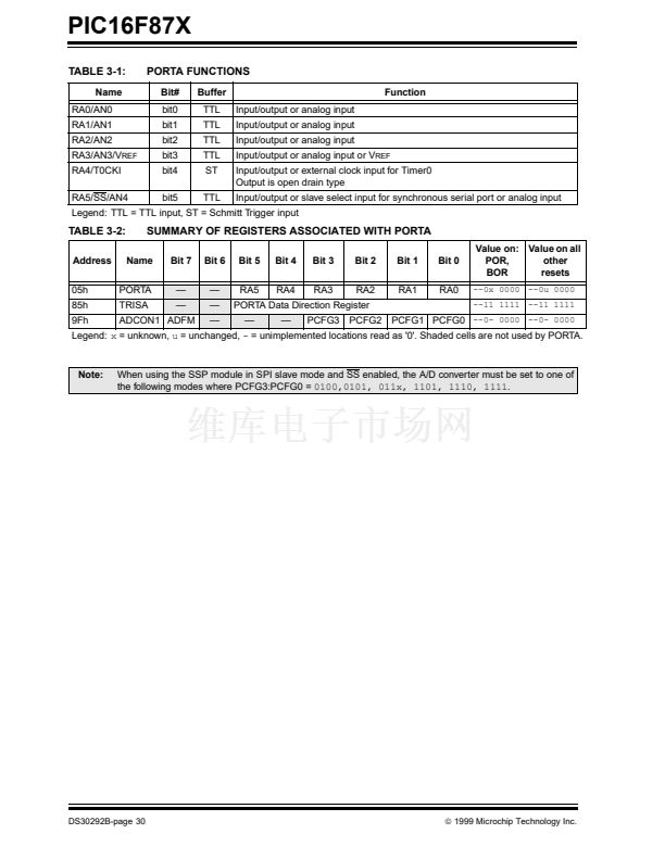
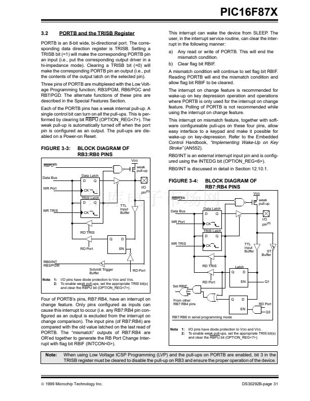
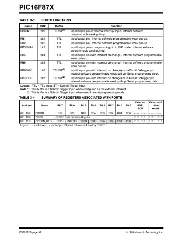
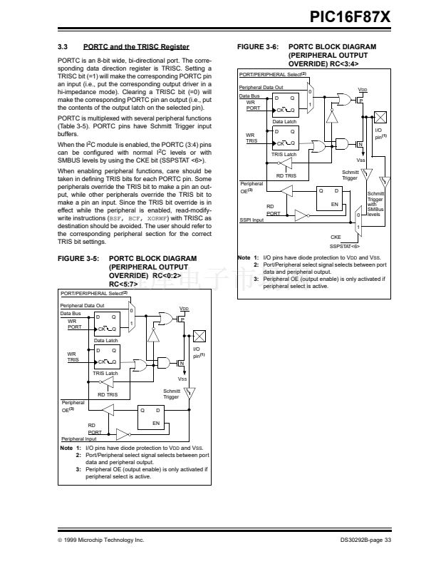
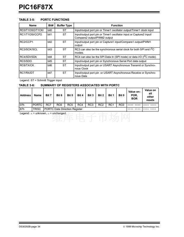
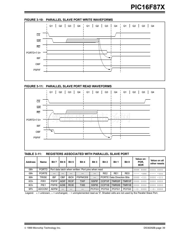
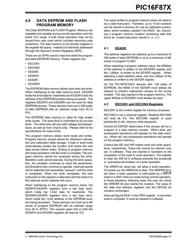
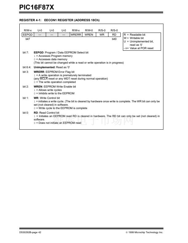
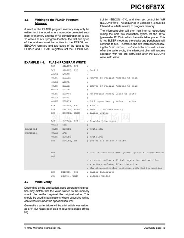
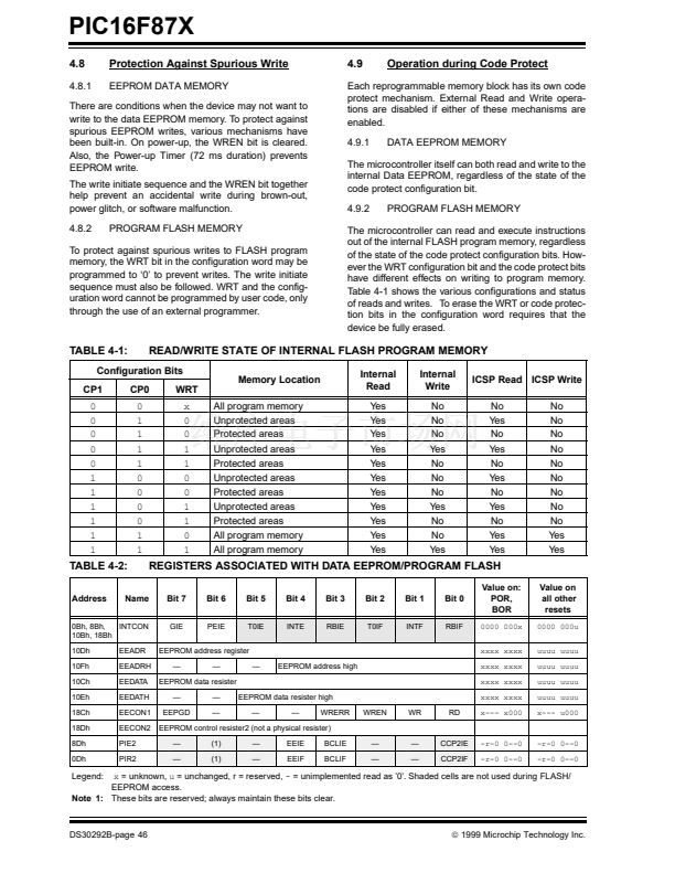
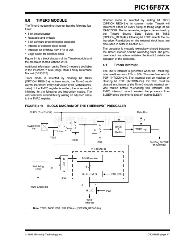
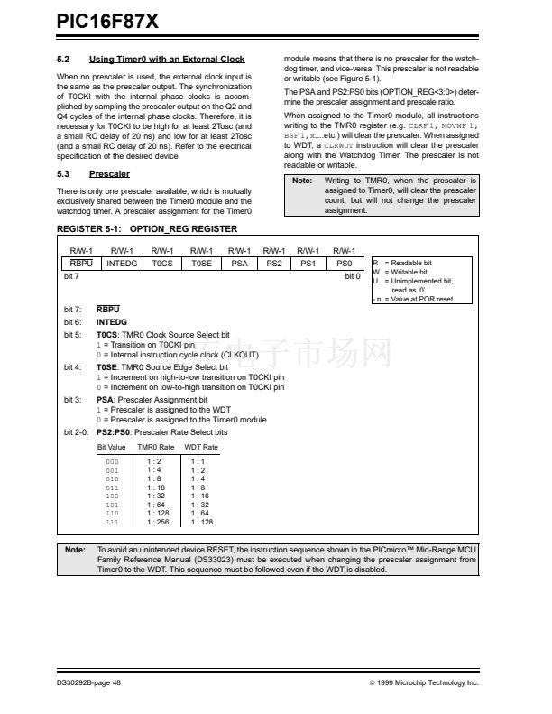
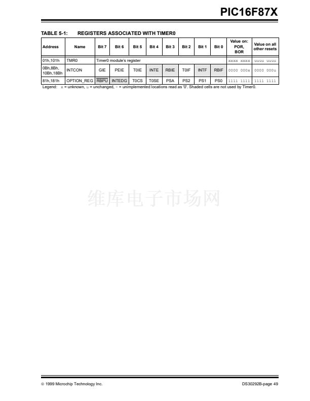
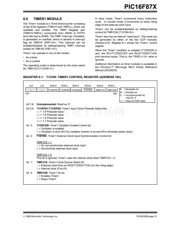
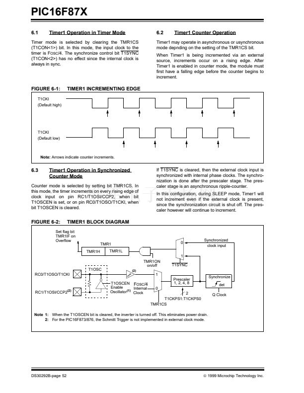
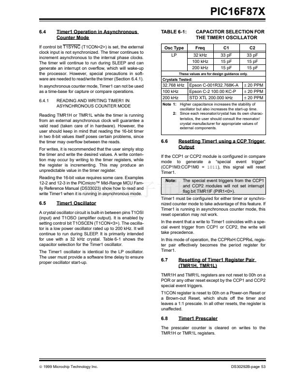
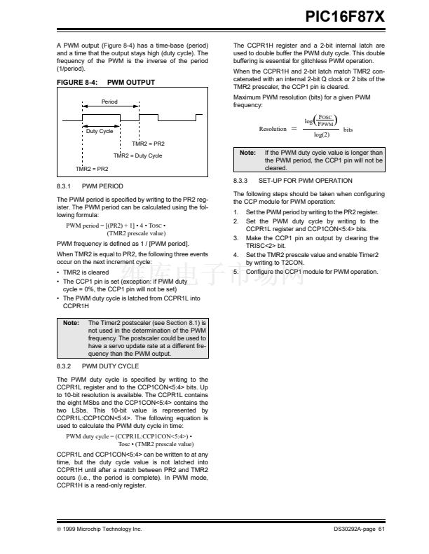
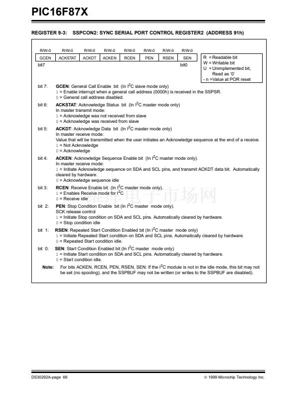
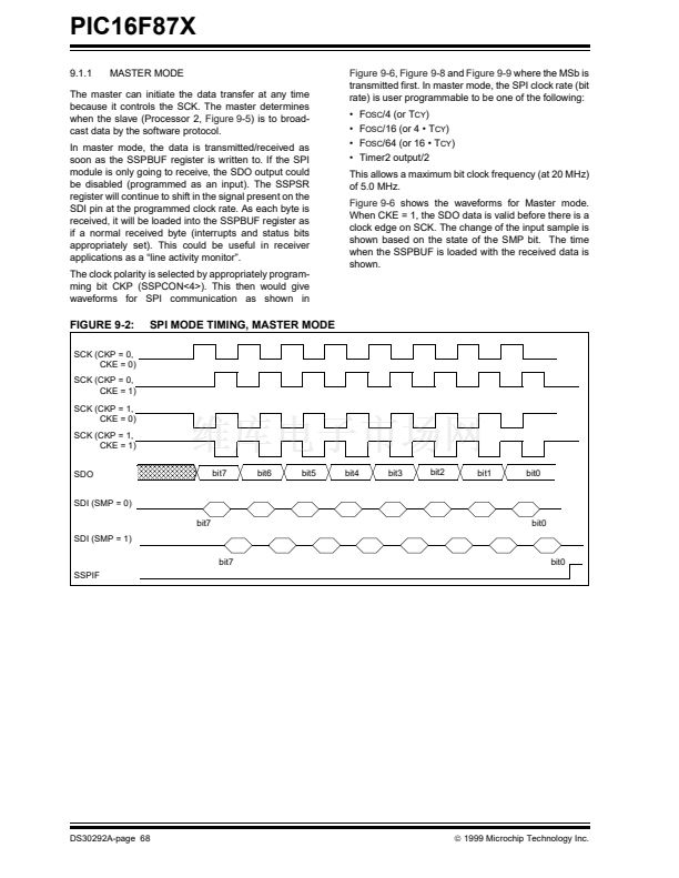
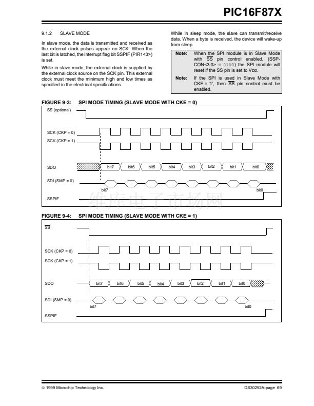
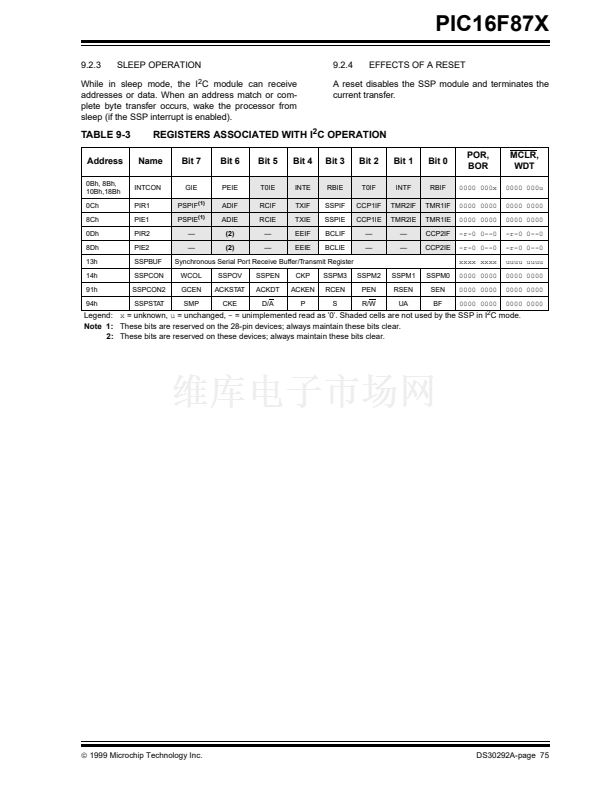
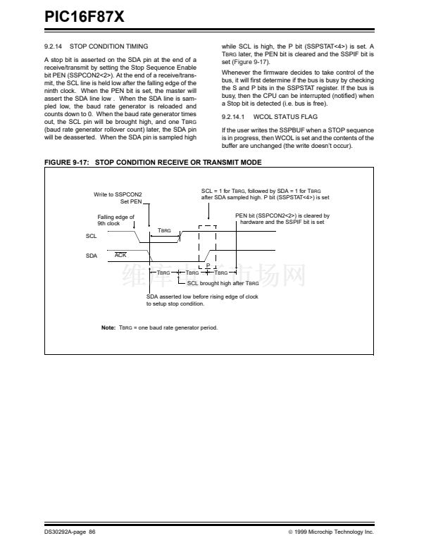
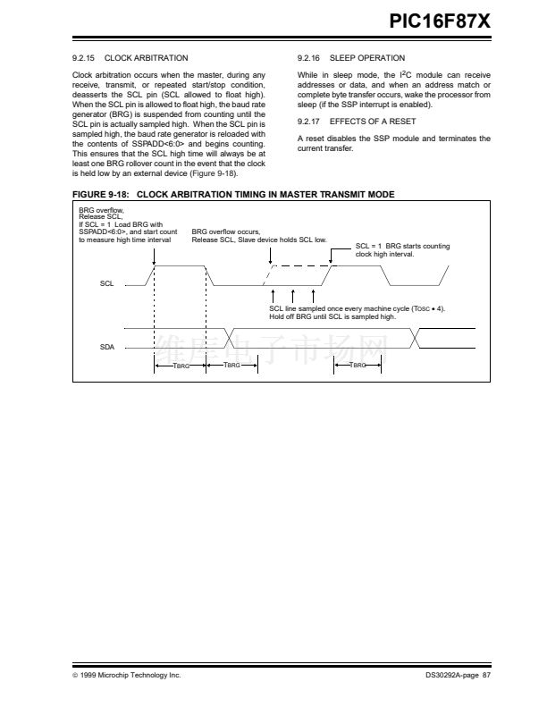
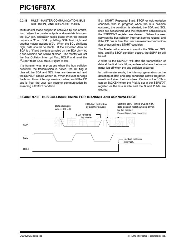
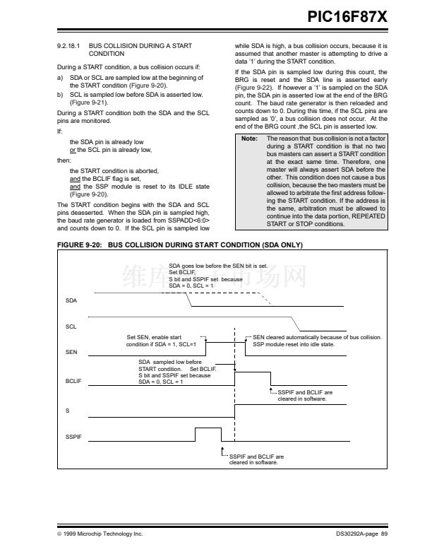
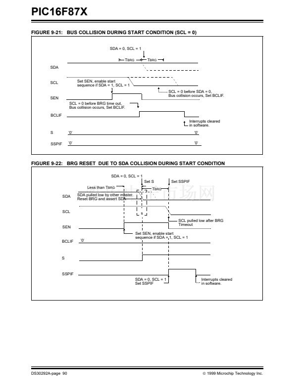
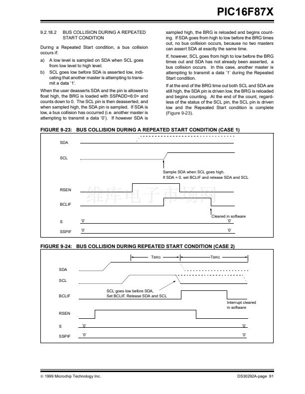
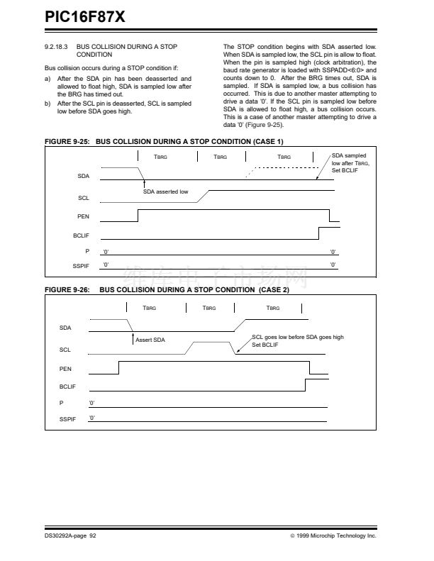
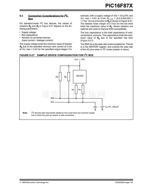
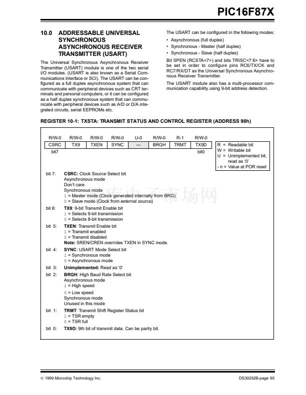
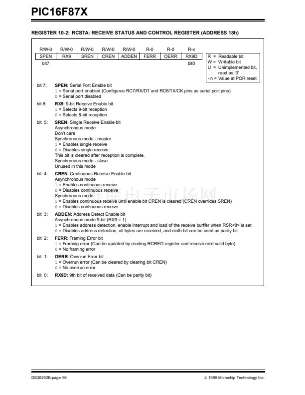
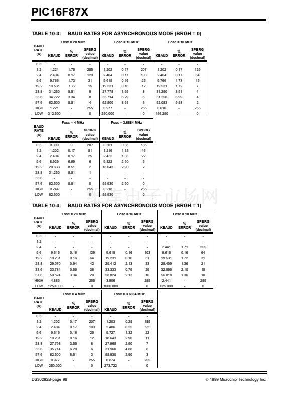
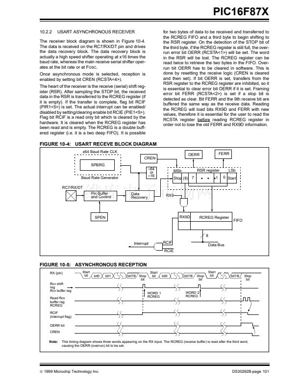
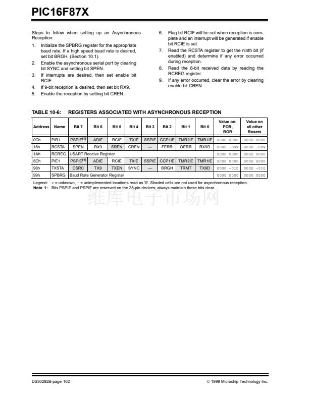
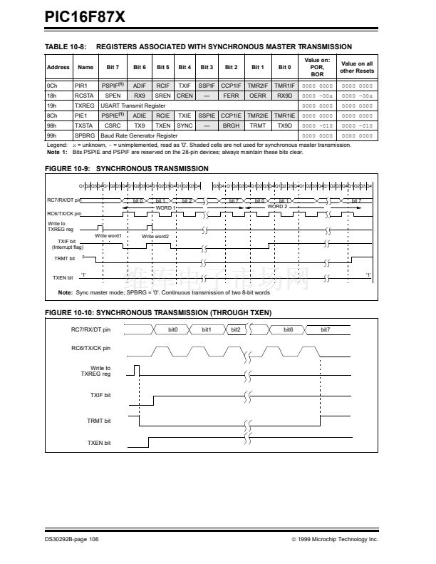
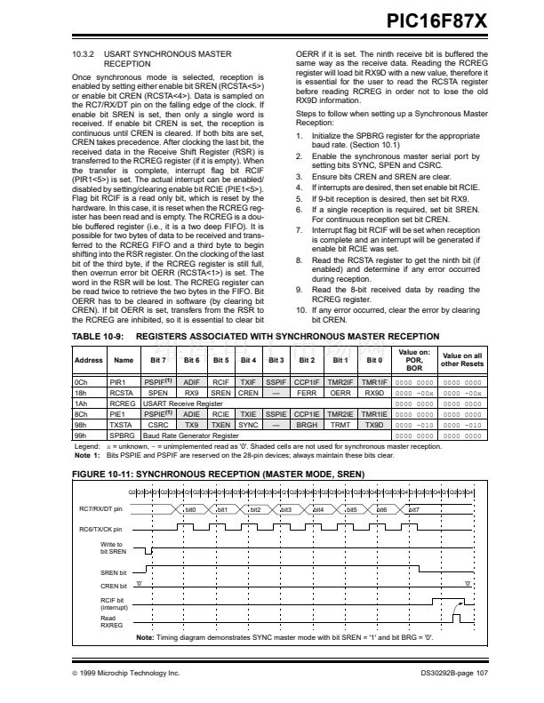
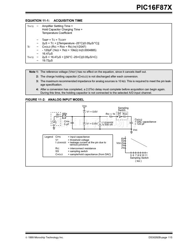
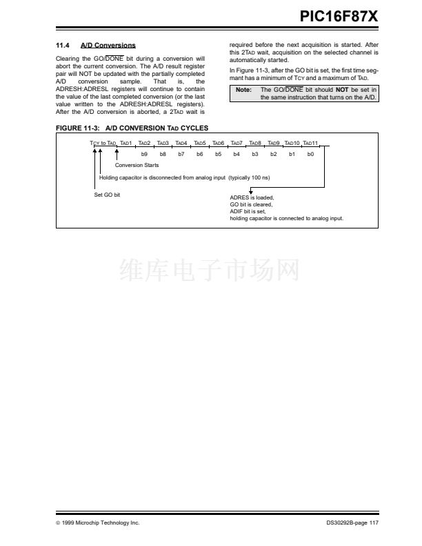
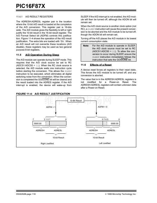
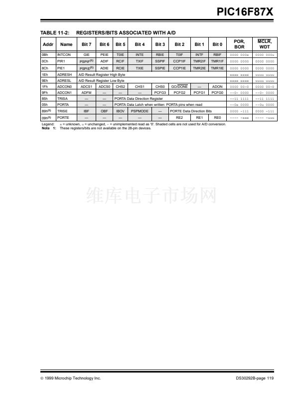
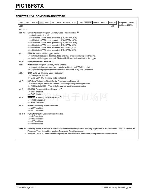
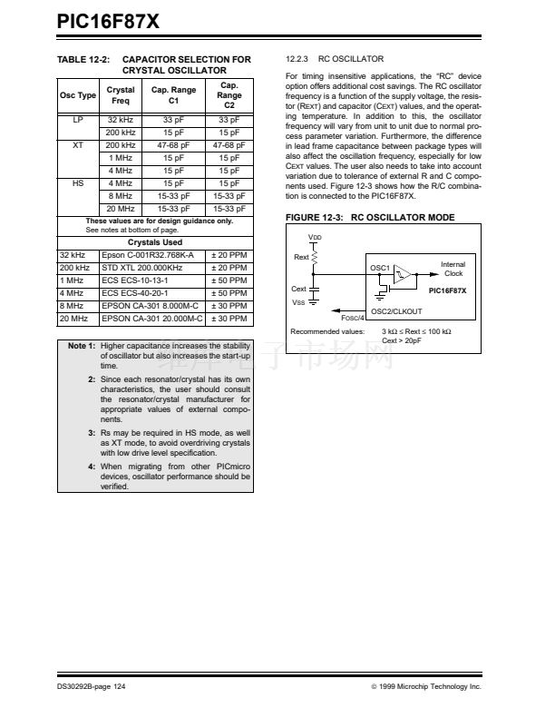
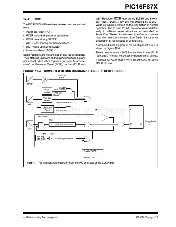
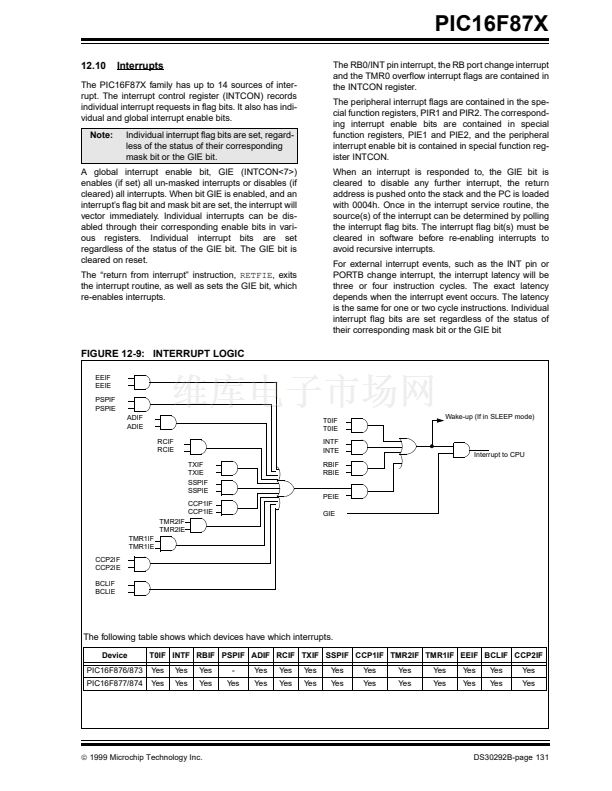
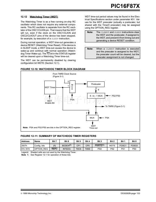
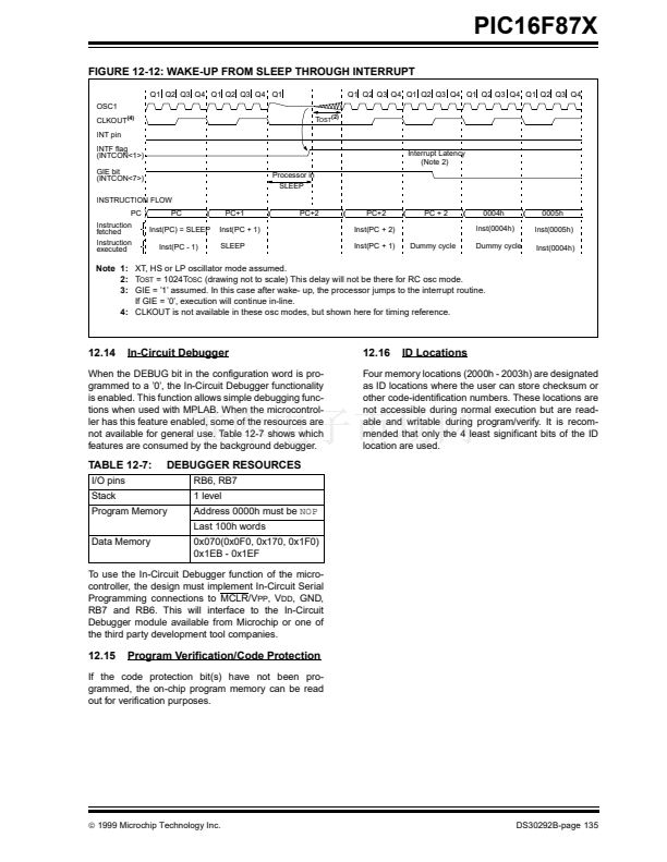
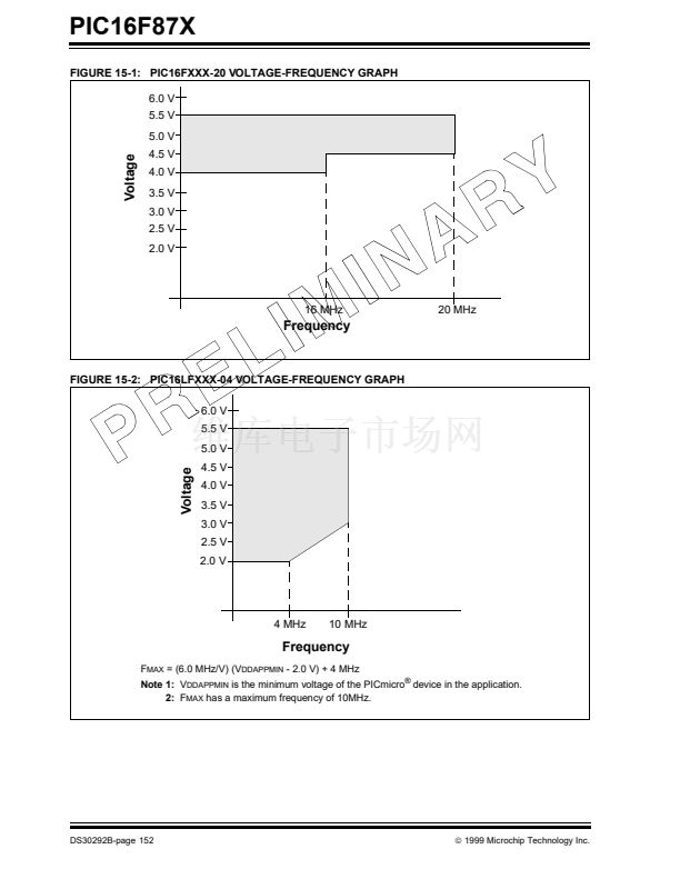
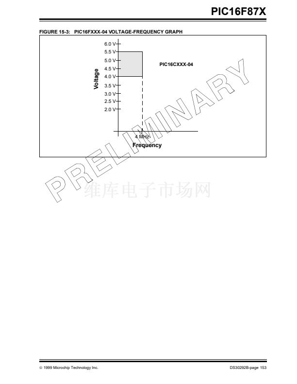
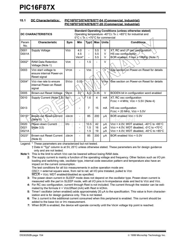
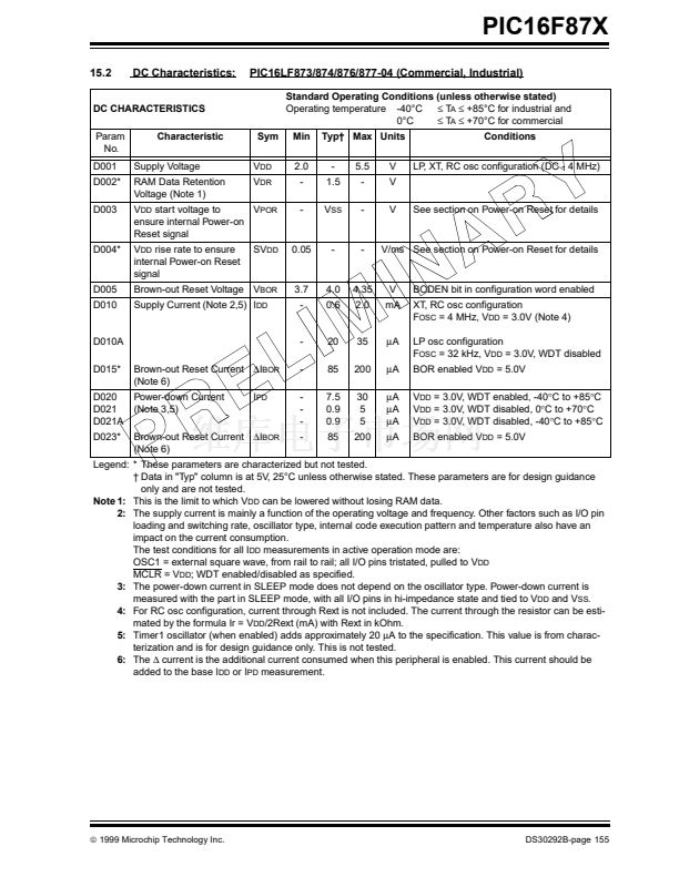
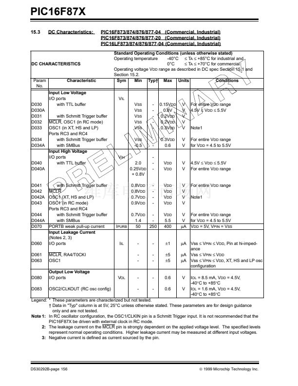
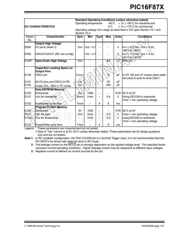
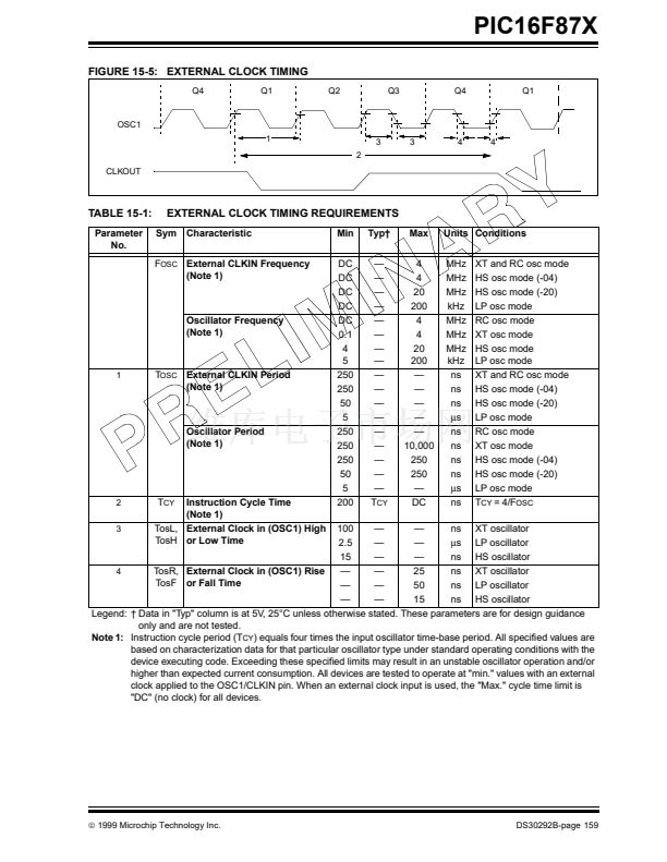
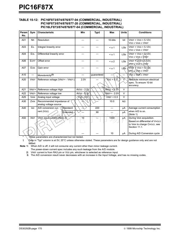
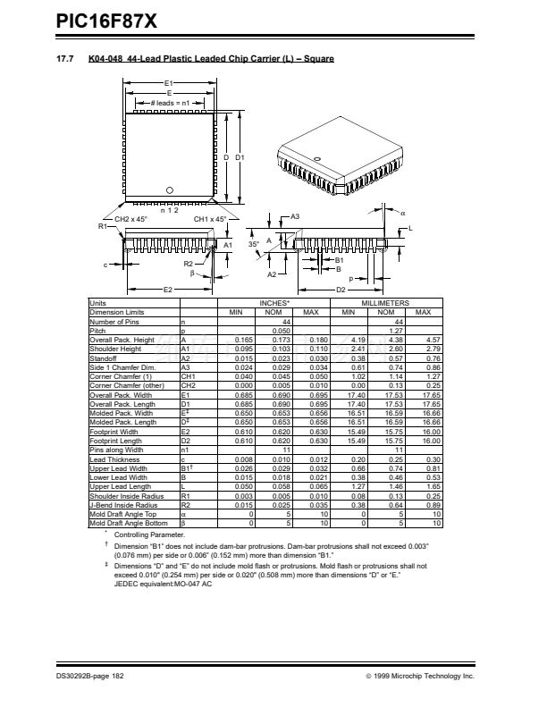
PIC16F87X
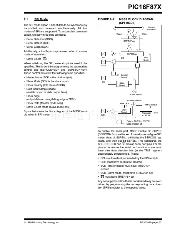
9.2
MSSP I
2
C Operation
The MSSP module in I
2
C mode fully implements all
master and slave functions (including general call sup-
port) and provides interrupts-on-start and stop bits in
hardware to determine a free bus (multi-master func-
tion). The MSSP module implements the standard
mode specifications, as well as 7-bit and 10-bit
addressing.
Refer to Application Note AN578,
"Use of the SSP
Module in the I
2
C Multi-Master Environment."
A "glitch" filter is on the SCL and SDA pins when the pin
is an input. This filter operates in both the 100 kHz and
400 kHz modes. In the 100 kHz mode, when these pins
are an output, there is a slew rate control of the pin that
is independant of device frequency.
Two pins are used for data transfer. These are the SCL
pin, which is the clock, and the SDA pin, which is the
data. The SDA and SCL pins are automatically config-
ured when the I
2
C mode is enabled. The SSP module
functions are enabled by setting SSP Enable bit
SSPEN (SSPCON<5>).
The MSSP module has six registers for I
2
C operation.
They are the:
SSP Control Register (SSPCON)
SSP Control Register2 (SSPCON2)
SSP Status Register (SSPSTAT)
Serial Receive/Transmit Buffer (SSPBUF)
SSP Shift Register (SSPSR) - Not directly acces-
sible
鈥?SSP Address Register (SSPADD)
The SSPCON register allows control of the I
2
C opera-
tion. Four mode selection bits (SSPCON<3:0>) allow
one of the following I
2
C modes to be selected:
鈥?I
2
C Slave mode (7-bit address)
鈥?I
2
C Slave mode (10-bit address)
鈥?I
2
C Master mode, clock = OSC/4 (SSPADD +1)
Before selecting any I
2
C mode, the SCL and SDA pins
must be programmed to inputs by setting the appropri-
ate TRIS bits. Selecting an I
2
C mode, by setting the
SSPEN bit, enables the SCL and SDA pins to be used
as the clock and data lines in I
2
C mode.
The CKE bit (SSPSTAT<6:7>) sets the levels of the
SDA and SCL pins in either master or slave mode.
When CKE = 1, the levels will conform to the SMBUS
specification. When CKE = 0, the levels will conform to
the I
2
C specification.
鈥?/div>
鈥?/div>
鈥?/div>
鈥?/div>
鈥?/div>
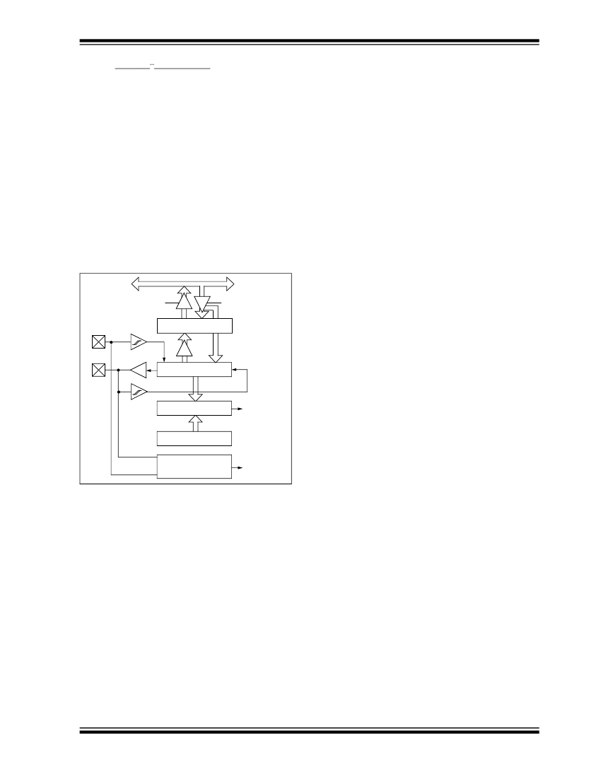
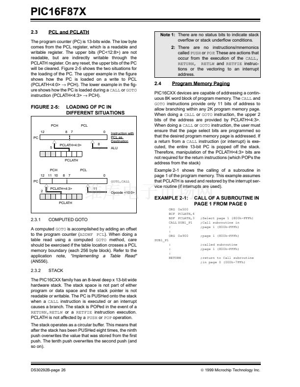
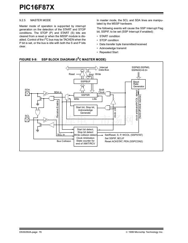
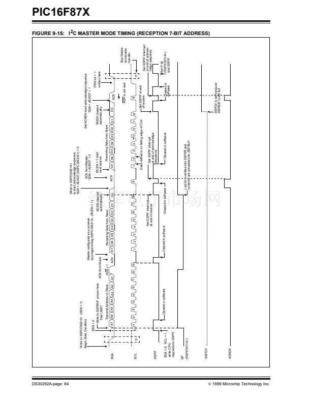
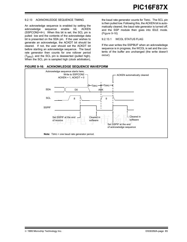
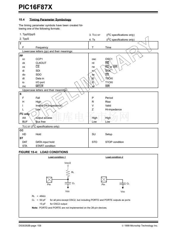
FIGURE 9-5:
I
2
C SLAVE MODE BLOCK
DIAGRAM
Internal
Data Bus
Read
SSPBUF reg
Shift
Clock
SSPSR reg
Write
SCL
SDA
MSb
LSb
Match detect
Addr Match
SSPADD reg
Start and
Stop bit detect
Set, Reset
S, P bits
(SSPSTAT reg)
漏
1999 Microchip Technology Inc.
DS30292A-page 71
PIC16F87X相关型号PDF文件下载
-
型号
版本
描述
厂商
下载
-
英文版
8-Pin FLASH-Based 8-Bit CMOS Microcontrollers
-
英文版
8-Pin, 8-Bit CMOS Microcontroller with EEPROM Data Memory
MICROCHIP ...
-
英文版
8-Pin, 8-Bit CMOS Microcontroller with A/D Converter and EEP...
MICROCHIP ...
-
英文版
8-Pin, 8-Bit CMOS Microcontrollers
MICROCHIP ...
-
英文版
EPROM Memory Programming Specification
MICROCHIP ...
-
英文版
8-Pin FLASH-Based 8-Bit CMOS Microcontrollers
MICROCHIP ...
-
英文版
Microcontroller
-
英文版
Microcontroller
-
英文版
Microcontroller
ETC
-
英文版
EPROM-Based 8-Bit CMOS Microcontroller
-
英文版
8-Pin, 8-Bit CMOS Microcontrollers
-
英文版
8-Pin, 8-Bit CMOS Microcontrollers
MICROCHIP ...
-
英文版
ETC
-
英文版
EPROM Memory Programming Specification
-
英文版
EPROM Memory Programming Specification
MICROCHIP ...
-
英文版
28-Pin Programmable Mixed Signal Controller
-
英文版
EPROM Memory Programming Specification
-
英文版
Microcontroller
ETC
-
英文版
Microcontroller
ETC
-
英文版
EPROM/ROM-Based 8-Bit CMOS Microcontroller Series


 1
1
 2
2
 3
3
 4
4
 5
5
 6
6
 7
7
 8
8
 9
9
 10
10
 11
11
 12
12
 13
13
 14
14
 15
15
 16
16
 17
17
 18
18
 19
19
 20
20
 21
21
 22
22
 23
23
 24
24
 25
25
 26
26
 27
27
 28
28
 29
29
 30
30
 31
31
 32
32
 33
33
 34
34
 35
35
 36
36
 37
37
 38
38
 39
39
 40
40
 41
41
 42
42
 43
43
 44
44
 45
45
 46
46
 47
47
 48
48
 49
49
 50
50
 51
51
 52
52
 53
53
 54
54
 55
55
 56
56
 57
57
 58
58
 59
59
 60
60
 61
61
 62
62
 63
63
 64
64
 65
65
 66
66
 67
67
 68
68
 69
69
 70
70
 71
71
 72
72
 73
73
 74
74
 75
75
 76
76
 77
77
 78
78
 79
79
 80
80
 81
81
 82
82
 83
83
 84
84
 85
85
 86
86
 87
87
 88
88
 89
89
 90
90
 91
91
 92
92
 93
93
 94
94
 95
95
 96
96
 97
97
 98
98
 99
99
 100
100
 101
101
 102
102
 103
103
 104
104
 105
105
 106
106
 107
107
 108
108
 109
109
 110
110
 111
111
 112
112
 113
113
 114
114
 115
115
 116
116
 117
117
 118
118
 119
119
 120
120
 121
121
 122
122
 123
123
 124
124
 125
125
 126
126
 127
127
 128
128
 129
129
 130
130
 131
131
 132
132
 133
133
 134
134
 135
135
 136
136
 137
137
 138
138
 139
139
 140
140
 141
141
 142
142
 143
143
 144
144
 145
145
 146
146
 147
147
 148
148
 149
149
 150
150
 151
151
 152
152
 153
153
 154
154
 155
155
 156
156
 157
157
 158
158
 159
159
 160
160
 161
161
 162
162
 163
163
 164
164
 165
165
 166
166
 167
167
 168
168
 169
169
 170
170
 171
171
 172
172
 173
173
 174
174
 175
175
 176
176
 177
177
 178
178
 179
179
 180
180
 181
181
 182
182
 183
183
 184
184
 185
185
 186
186
 187
187
 188
188
 189
189
 190
190
 191
191
 192
192
 193
193
 194
194
 195
195
 196
196
 197
197
 198
198
 199
199
 200
200
