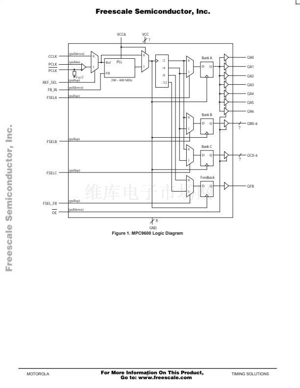
鈩?/div>
VTT
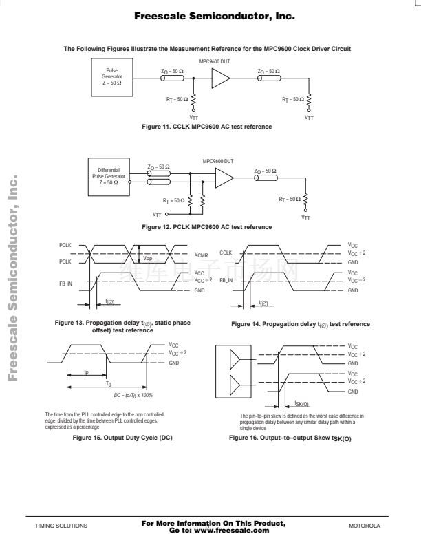
Figure 12. PCLK MPC9600 AC test reference
PCLK
PCLK
VPP
VCMR
VCC
VCC 2
CCLK
VCC
VCC 2
B
B
GND
FB_IN
t(鈭?
B
FB_IN
VCC
VCC 2
GND
t(鈭?
GND
Figure 13. Propagation delay t
(鈭?
, static phase
offset) test reference
VCC
VCC 2
Figure 14. Propagation delay t
(鈭?
test reference
VCC
VCC 2
B
B
B
GND
tP
T0
DC = tP /T0
x
100%
tSK(O)
The time from the PLL controlled edge to the non controlled
edge, divided by the time between PLL controlled edges,
expressed as a percentage
GND
VCC
VCC 2
GND
The pin鈥搕o鈥損in skew is defined as the worst case difference in
propagation delay between any similar delay path within a
single device
Figure 15. Output Duty Cycle (DC)
Figure 16. Output鈥搕o鈥搊utput Skew tSK(O)
TIMING SOLUTIONS
For More Information On This Product,
11
Go to: www.freescale.com
MOTOROLA


 1
1
 2
2
 3
3
 4
4
 5
5
 6
6
 7
7
 8
8
 9
9
 10
10
 11
11
 12
12
 13
13
 14
14
 15
15
 16
16
