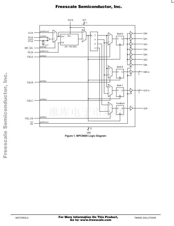
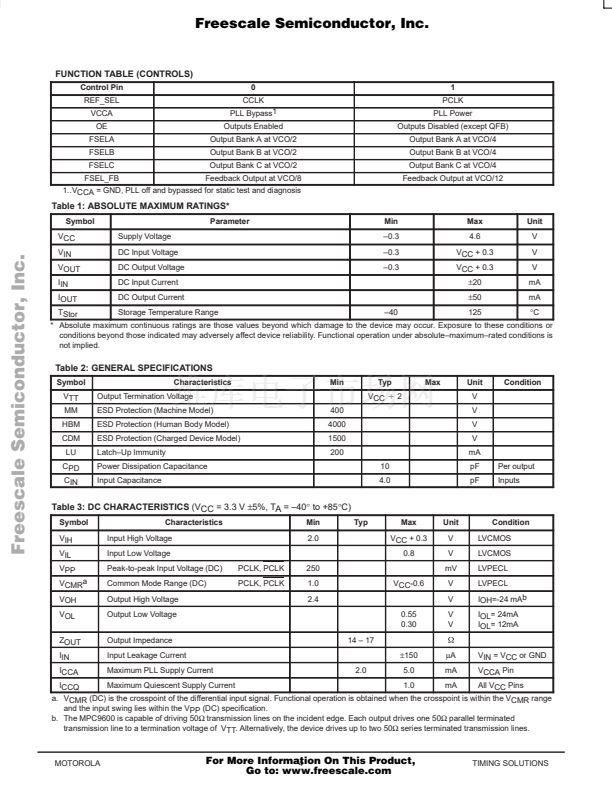
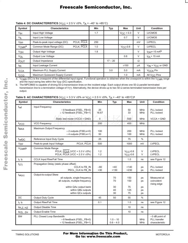
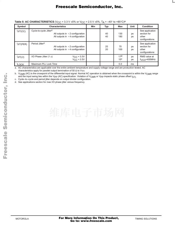
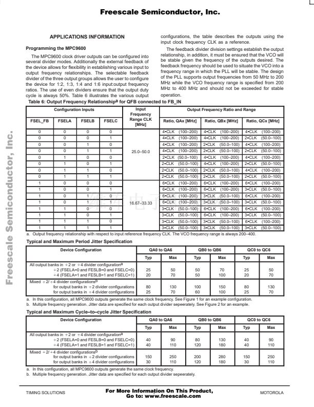
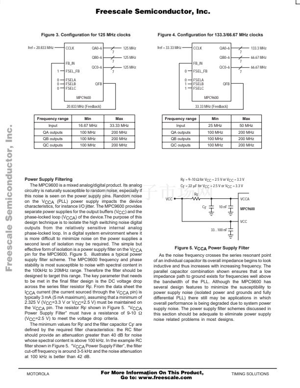
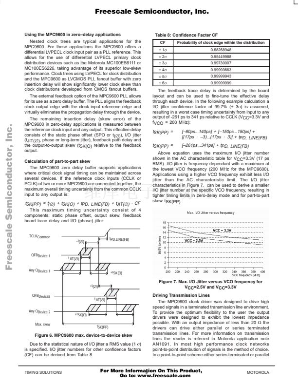
Freescale Semiconductor, Inc.
PIN CONFIGURATION
Pin
PCLK, PCLK
CCLK
FB_IN
QAn
QBn
QCn
QFB
REF_SEL
I/O
Input
Input
Input
Output
Output
Output
Output
Input
Input
Input
Input
Input
Input
Type
PECL
LVCMOS
LVCMOS
LVCMOS
LVCMOS
LVCMOS
LVCMOS
LVCMOS
LVCMOS
LVCMOS
LVCMOS
LVCMOS
LVCMOS
Power supply
Power supply
Ground
GND
QFB
Description
Differential reference clock frequency input
Reference clock input
PLL feedback clock input
Bank A outputs
Bank B outputs
Bank C outputs
Differential feedback output
Reference clock input select
Selection of bank A output frequency
Selection of bank B output frequency
Selection of bank C output frequency
Selection of feedback frequency
Output enable
Analog power supply and PLL bypass. An external VCC filter is recommended for VCCA
Core power supply
Ground
GND
VCC
VCC
25
24
23
22
21
20
19
GND
QC0
QC1
QC2
VCC
QC3
QC4
GND
QC5
QC6
OE
VCC
18
17
16
15
14
13
1
2
3
4
5
6
7
8
9
10
11
12
GND
QB0
QB1
QB2
QB3
QB4
QB5
27
FSELB
QB6
26
FSELC
Freescale Semiconductor, Inc...
FSELA
FSELB
FSELC
FSEL_FB
OE
VCCA
VCC
GND
36
VCC
QA6
QA5
QA4
GND
QA3
QA2
VCC
QA1
QA0
FB_IN
GND
37
38
39
40
41
42
35
34
33
32
31
30
29
28
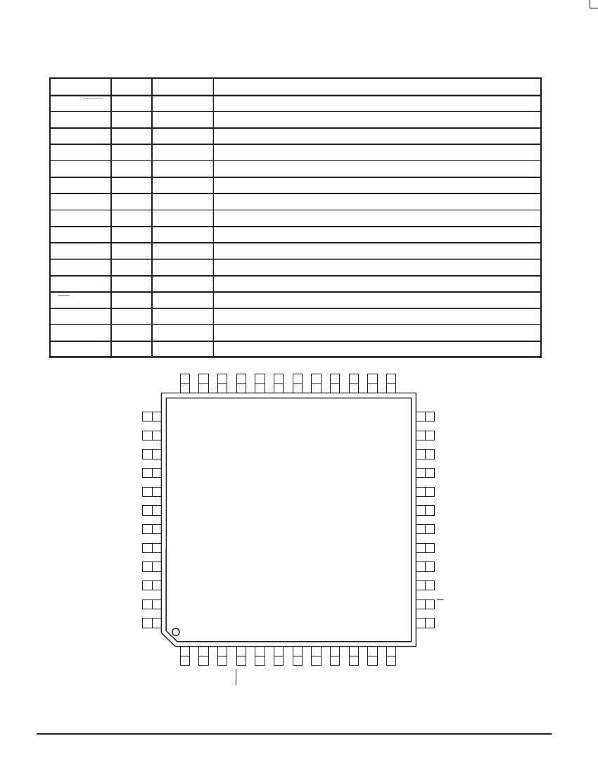
MPC9600
43
44
45
46
47
48
CCLK
REF_SEL
FSEL_FB
VCCA
PCLK
PCLK
GND
VCC
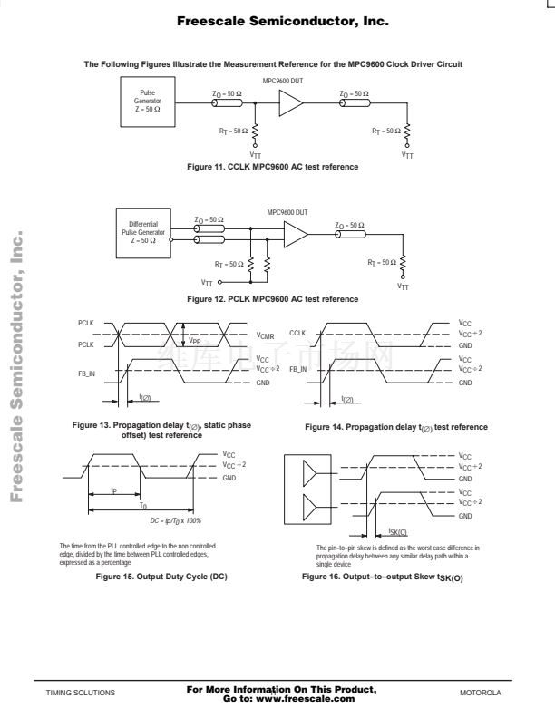
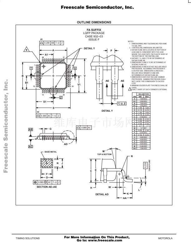
Figure 2. 48 Lead Package Pinout
(Top View)
TIMING SOLUTIONS
For More Information On This Product,
3
Go to: www.freescale.com
FSELA
MOTOROLA


 1
1
 2
2
 3
3
 4
4
 5
5
 6
6
 7
7
 8
8
 9
9
 10
10
 11
11
 12
12
 13
13
 14
14
 15
15
 16
16
