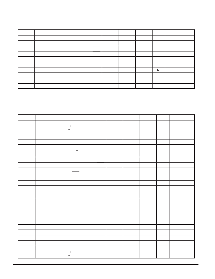
transmission line to a termination voltage of VTT. Alternatively, the device drives up to two 50
鈩?/div>
series terminated transmission lines per
output.
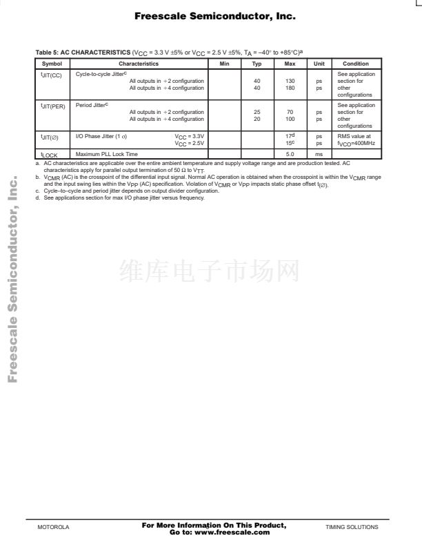
Table 5: AC CHARACTERISTICS
(VCC = 3.3 V
卤5%
or VCC = 2.5 V
卤5%,
TA = 鈥?0掳 to +85掳C)
a
Symbol
fref
Input Frequency
Characteristics
Min
25
16.67
0
200
Typ
Max
50
33
500
400
200
100
75
1000
VCC-0.8
VCC-0.6
1.0
鈥?0
+30
+40
+130
70
70
30
40
30
45
0.1
50
+140
+230
150
150
75
125
75
55
1.0
10
10
Unit
MHz
MHz
MHz
MHz
MHz
MHz
%
mV
V
V
ns
ps
ps
ps
ps
ps
ps
ps
%
ns
ns
ns
MHz
MHz
鈥? dB point of
PLL transfer
characteristic
see Figure 12
LVPECL
LVPECL
LVPECL
see Figure 12
PLL locked
PLL locked
Measured at
coincident
rising edge
PLL locked
PLL locked
Condition
PLL locked
PLL locked
VCCA = GND
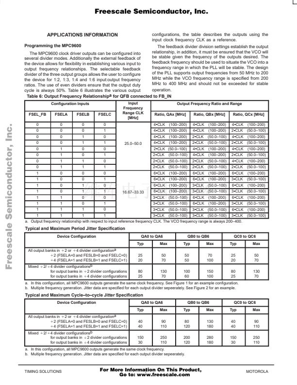
B
8 feedback (FSEL_FB=0)
B
12 feedback (FSEL_FB=1)
Static test mode (VCCA = GND)
fVCO
fMAX
VCO Frequency
Maximum Output Frequency
B
2 outputs (FSELx=0)
B
4 outputs (FSELx=1)
PCLK, PCLK
100
50
25
500
1.2
1.2
frefDC
VPP
VCMRb
Reference Input Duty Cycle
Peak-to-peak Input Voltage
Common Mode Range
PCLK, PCLK (VCC = 3.3 V
卤5%)
PCLK, PCLK (VCC = 2.5 V
卤5%)
CCLK Input Rise/Fall Time
Propagation Delay (static phase offset)
CCLK to FB_IN
PECL_CLK to FB_IN
Output-to-output Skew
all outputs, single frequency
all outputs, multiple frequency
within QAx output bank
within QBx outputs
within QCx outputs
tr, tf
t(鈭?
tsk(o)
DC
tr, tf
tPLZ, HZ
tPZL, ZH
BW
Output Duty Cycle
Output Rise/Fall Time
Output Disable Time
Output Enable Time
PLL Closed Loop Bandwidth
8 feedback (FSEL_FB=0)
12 feedback (FSEL_FB=1)
B
B
1.0 鈥?10
0.6 鈥?4.0
TIMING SOLUTIONS
For More Information On This Product,
5
Go to: www.freescale.com
MOTOROLA


 1
1
 2
2
 3
3
 4
4
 5
5
 6
6
 7
7
 8
8
 9
9
 10
10
 11
11
 12
12
 13
13
 14
14
 15
15
 16
16
