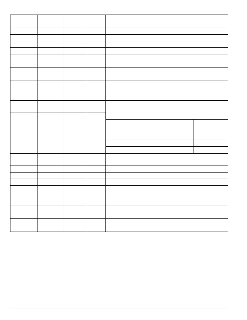
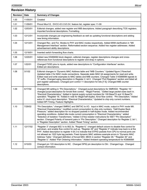
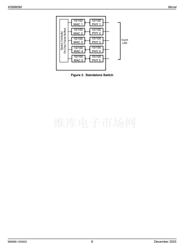
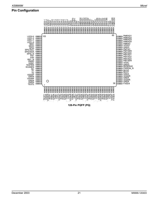
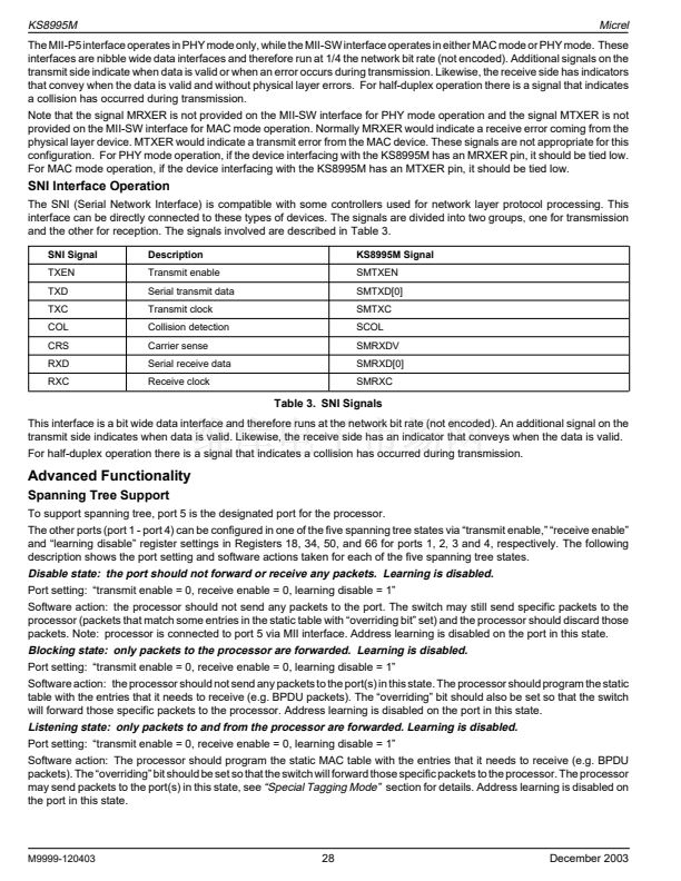
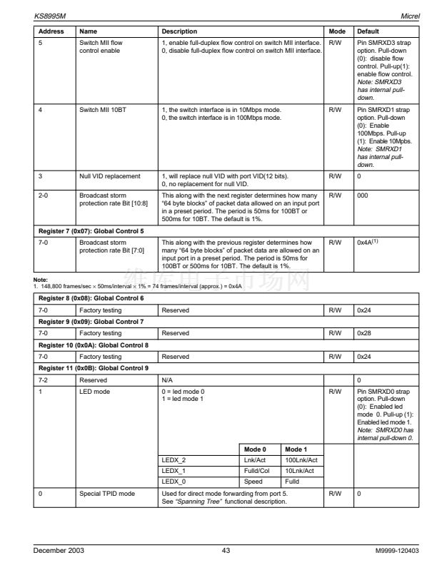
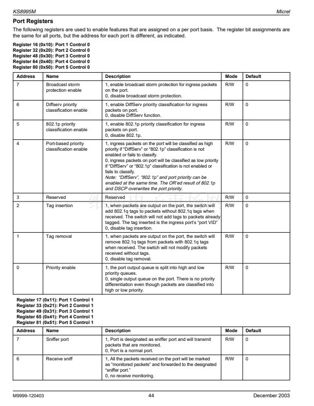
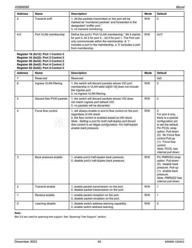
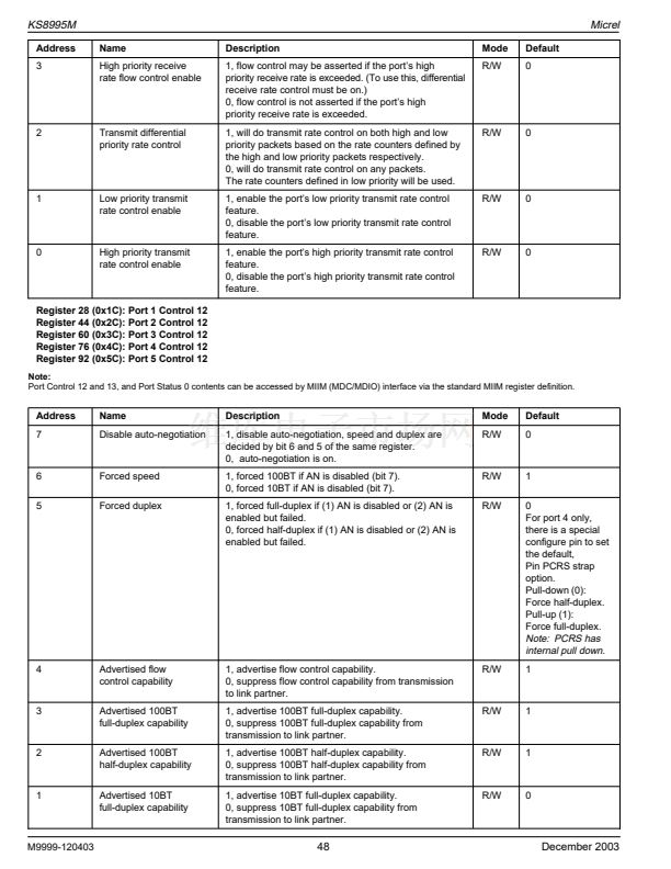
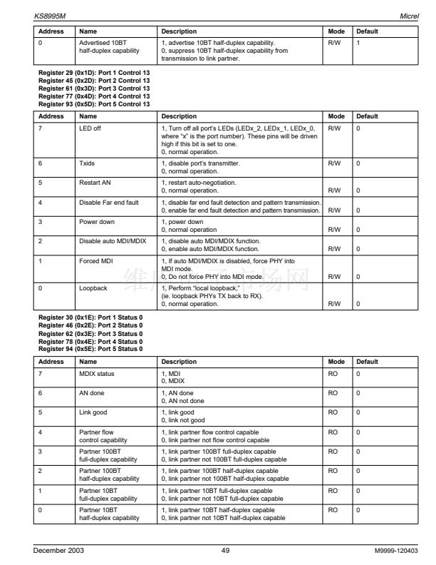
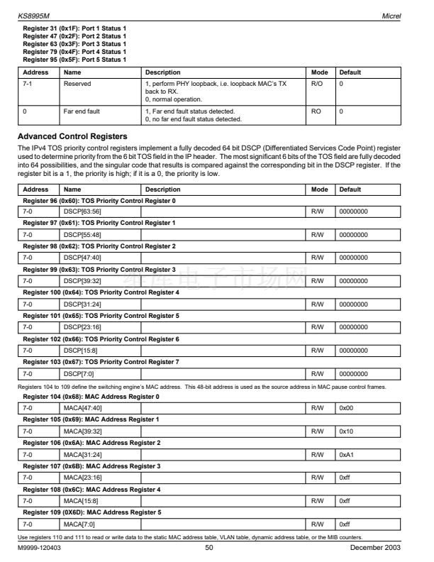
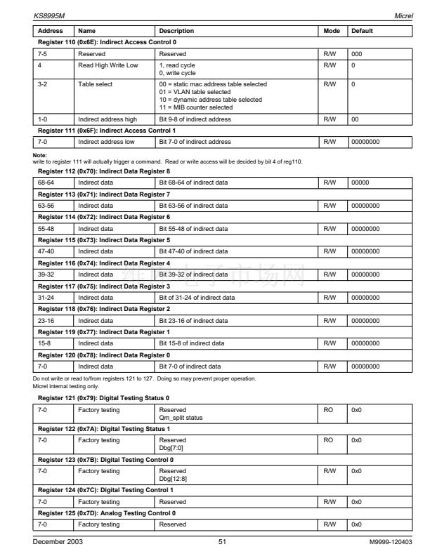
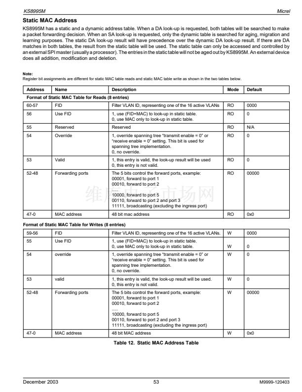
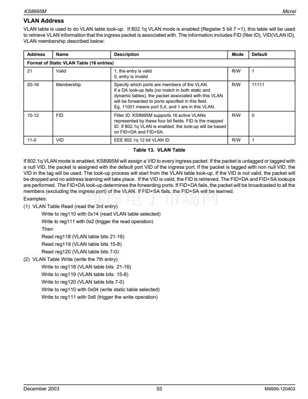
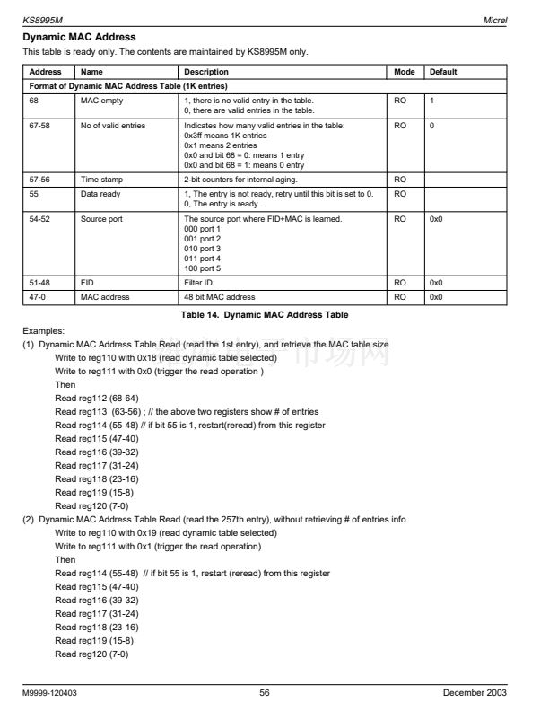
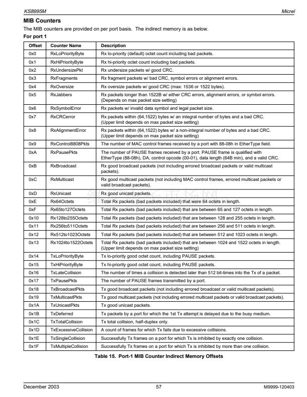
KS8995M
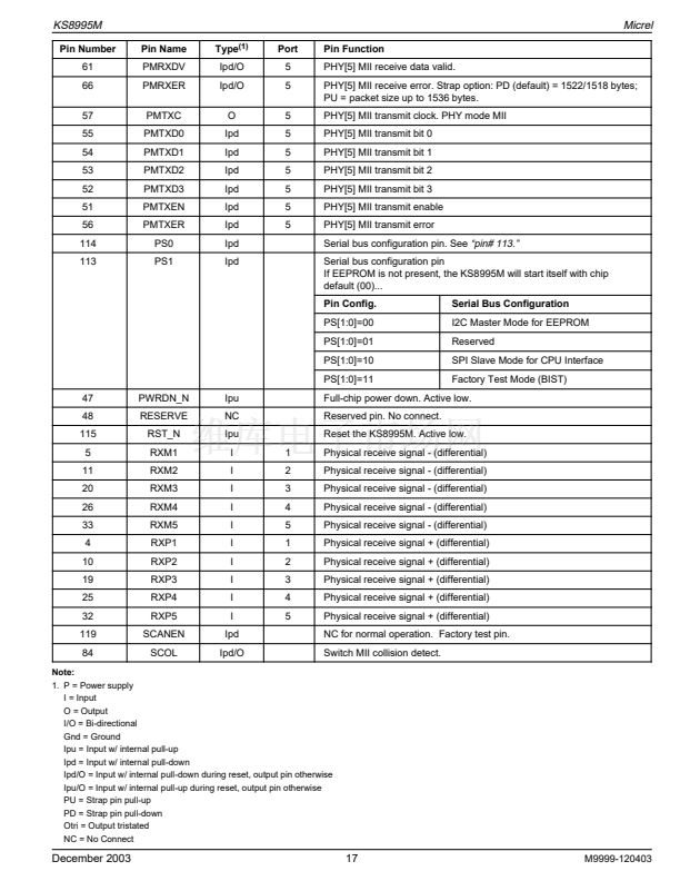
Pin Number
32
33
34
35
36
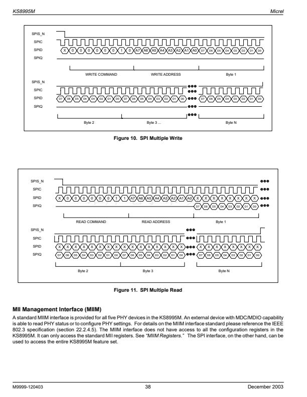
37
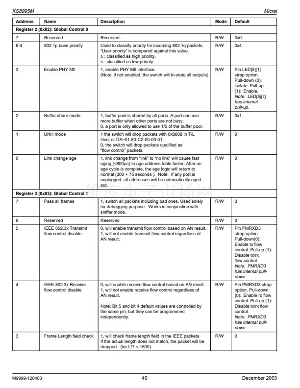
38
39
40
41
42
43
44
45
46
Pin Name
RXP5
RXM5
GNDA
TXM5
TXP5
VDDAT
FXSD5
FXSD4
GNDA
VDDAR
GNDA
VDDAR
GNDA
MUX1
MUX2
Type
(1)
I
I
Gnd
O
O
P
I
I
Gnd
P
Gnd
P
Gnd
NC
NC
5
4
5
5
Port
5
5
Pin Function
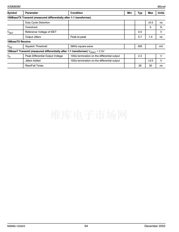
Physical receive signal + (differential)
Physical receive signal - (differential)
Analog ground
Physical transmit signal - (differential)
Physical transmit signal + (differential)
2.5V analog V
DD
Fiber signal detect/factory test pin
Fiber signal detect/factory test pin
Analog ground
1.8V analog V
DD
Analog ground
1.8V analog V
DD
Analog ground
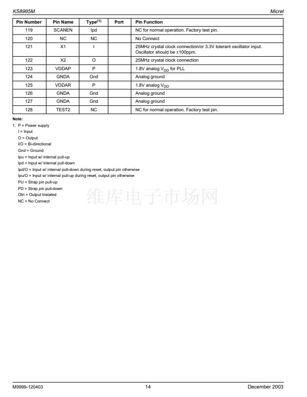
MUX1 and MUX2 should be left unconnected for normal operation.
They are factory test pins.
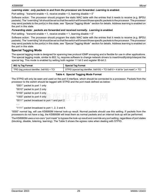
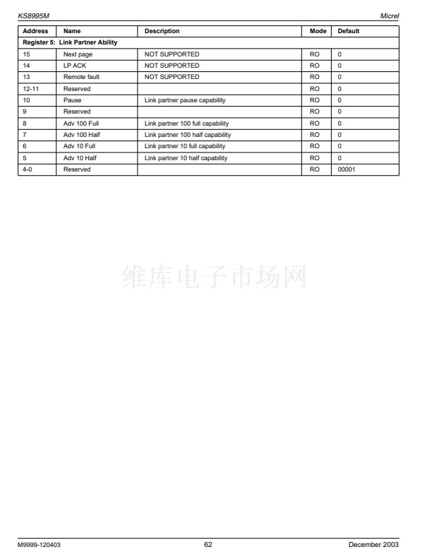
Mode
Normal Operation
Remote Analog Loopback Mode for Testing only
Reserved
Power Save Mode for Testing only
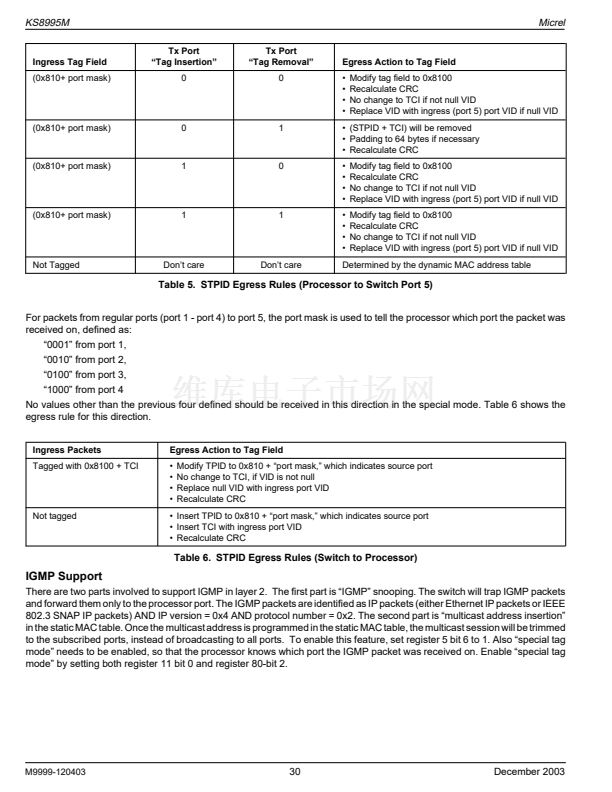
47
48
49
50
51
52
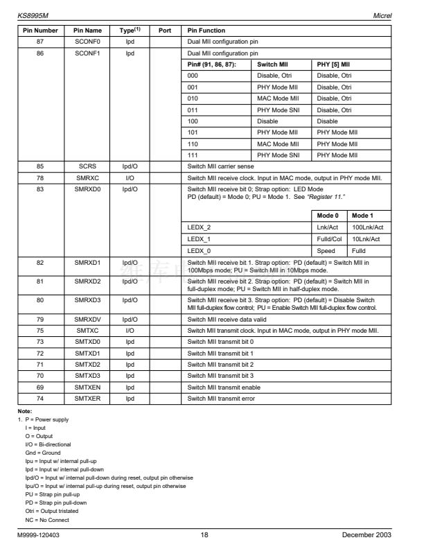
53
54
55
56
57
58
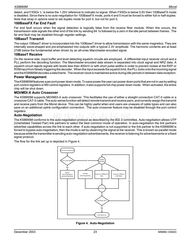
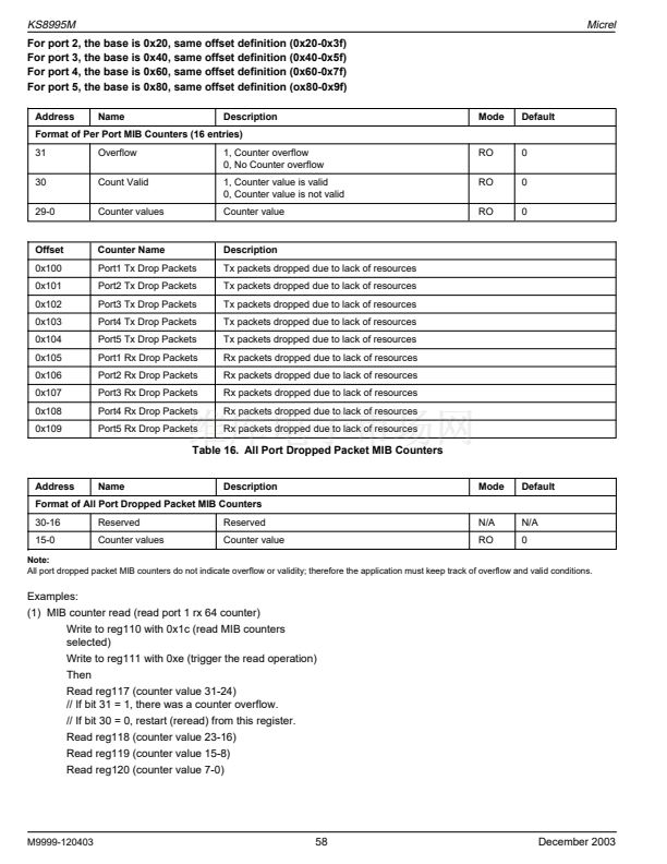
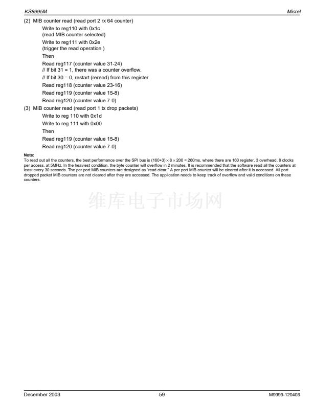
Note:
1. P = Power supply
I = Input
O = Output
I/O = Bi-directional
Gnd = Ground
Ipu = Input w/ internal pull-up
Ipd = Input w/ internal pull-down
Ipd/O = Input w/ internal pull-down during reset, output pin otherwise
Ipu/O = Input w/ internal pull-up during reset, output pin otherwise
PU = Strap pin pull-up
PD = Strap pin pull-down
Otri = Output tristated
NC = No Connect
Micrel
Mux1
NC
0
1
1
Mux2
NC
1
0
1
PWRDN_N
RESERVE
GNDD
VDDC
PMTXEN
PMTXD3
PMTXD2
PMTXD1
PMTXD0
PMTXER
PMTXC
GNDD
Ipu
NC
Gnd
P
Ipd
Ipd
Ipd
Ipd
Ipd
Ipd
O
Gnd
5
5
5
5
5
5
5
Full-chip power down. Active low.
Reserved pin. No connect.
Digital ground
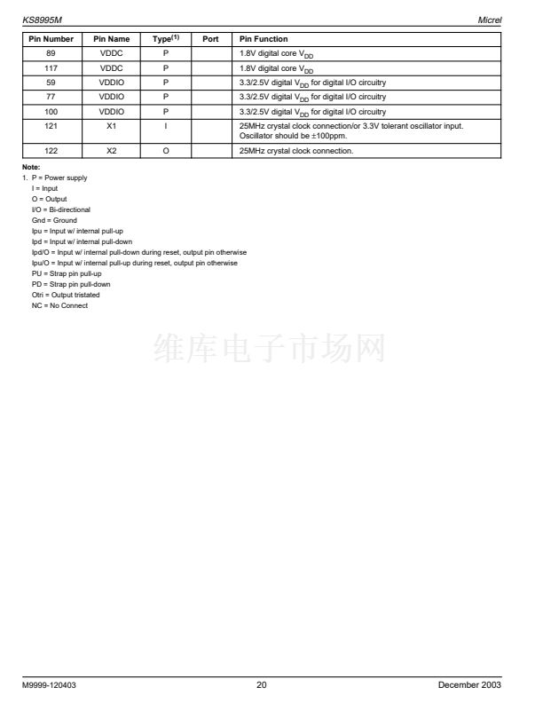
1.8V digital core V
DD
PHY[5] MII transmit enable
PHY[5] MII transmit bit 3
PHY[5] MII transmit bit 2
PHY[5] MII transmit bit 1
PHY[5] MII transmit bit 0
PHY[5] MII transmit error
PHY[5] MII transmit clock. PHY mode MII.
Digital ground
M9999-120403
10
December 2003


 1
1
 2
2
 3
3
 4
4
 5
5
 6
6
 7
7
 8
8
 9
9
 10
10
 11
11
 12
12
 13
13
 14
14
 15
15
 16
16
 17
17
 18
18
 19
19
 20
20
 21
21
 22
22
 23
23
 24
24
 25
25
 26
26
 27
27
 28
28
 29
29
 30
30
 31
31
 32
32
 33
33
 34
34
 35
35
 36
36
 37
37
 38
38
 39
39
 40
40
 41
41
 42
42
 43
43
 44
44
 45
45
 46
46
 47
47
 48
48
 49
49
 50
50
 51
51
 52
52
 53
53
 54
54
 55
55
 56
56
 57
57
 58
58
 59
59
 60
60
 61
61
 62
62
 63
63
 64
64
 65
65
 66
66
 67
67
 68
68
 69
69
 70
70
 71
71
 72
72
 73
73
