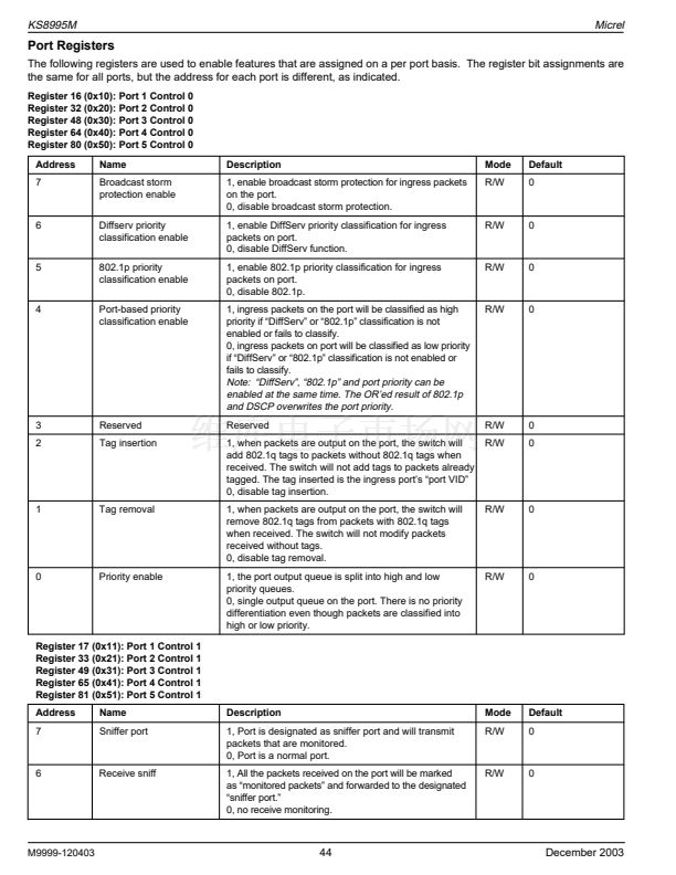
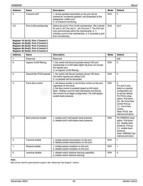
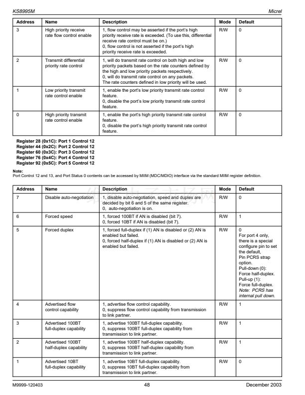
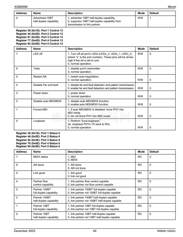
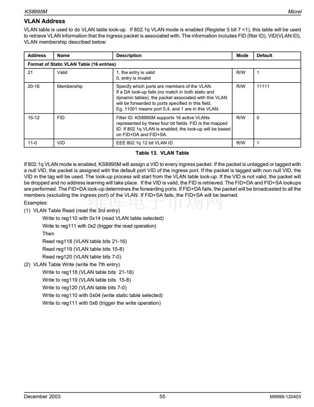
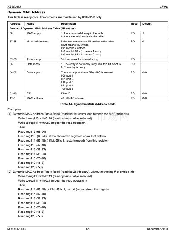
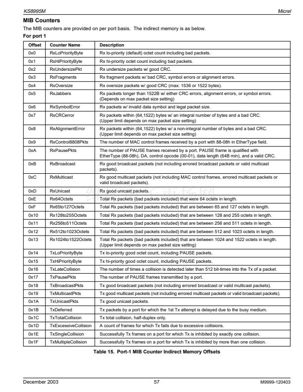
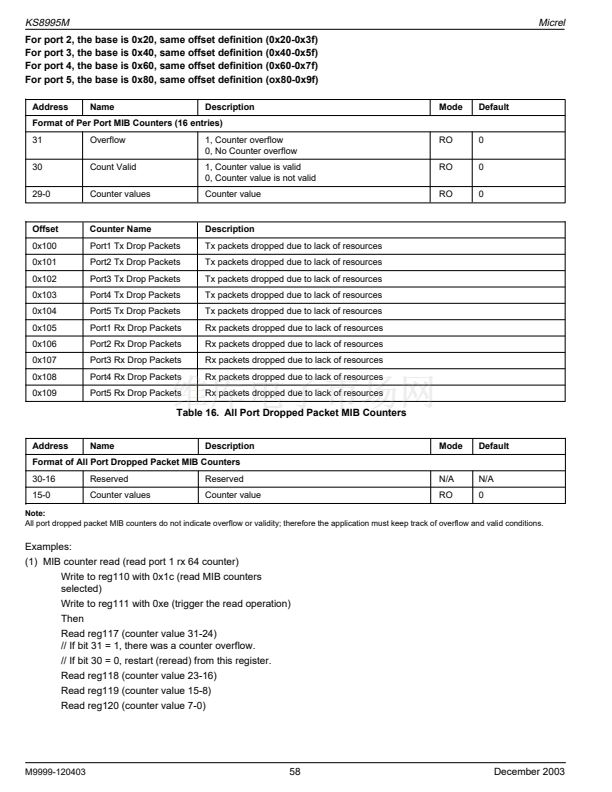
KS8995M
Micrel
Pin Description (by Number)
Pin Number
1
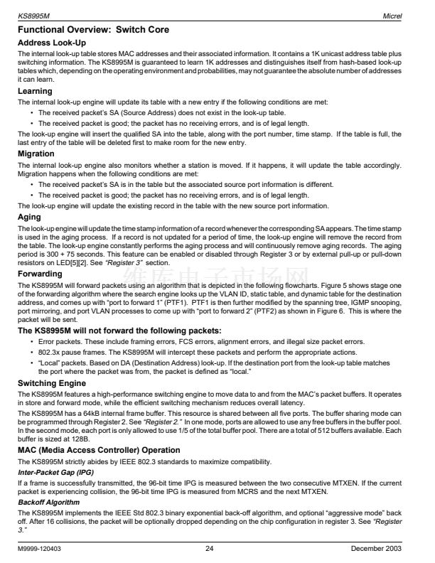
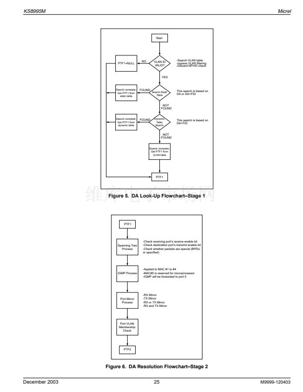
2
3
4
5
6
7
8
9
10
11
12
13
14
15
16
17
18
19
20
21
22
23
24
25
26
27
28
29
30
31
Note:
1. P = Power supply
I = Input
O = Output
I/O = Bi-directional
Gnd = Ground
Ipu = Input w/ internal pull-up
Ipd = Input w/ internal pull-down
Ipd/O = Input w/ internal pull-down during reset, output pin otherwise
Ipu/O = Input w/ internal pull-up during reset, output pin otherwise
PU = Strap pin pull-up
PD = Strap pin pull-down
Otri = Output tristated
NC = No Connect
Pin Name
TEST1
GNDA
VDDAR
RXP1
RXM1
GNDA
TXM1
TXP1
VDDAT
RXP2
RXM2
GNDA
TXM2
TXP2
VDDAR
GNDA
ISET
VDDAT
RXP3
RXM3
GNDA
TXM3
TXP3
VDDAT
RXP4
RXM4
GNDA
TXM4
TXP4
GNDA
VDDAR
Type
(1)
NC
Gnd
P
I
I
Gnd
O
O
P
I
I
Gnd
O
O
P
Gnd
Port
Pin Function
NC for normal operation. Factory test pin.
Analog ground
1.8V analog V
DD
1
1
Physical receive signal + (differential)
Physical receive signal - (differential)
Analog ground
1
1
Physical transmit signal - (differential)
Physical transmit signal + (differential)
2.5V analog V
DD
2
2
Physical receive signal + (differential)
Physical receive signal - (differential)
Analog ground
2
2
Physical transmit signal - (differential)
Physical transmit signal + (differential)
1.8V analog V
DD
Analog ground
Set physical transmit output current. Pull-down with a 3.01k鈩?1%
resistor.
P
I
I
Gnd
O
O
P
I
I
Gnd
O
O
Gnd
P
4
4
4
4
3
3
3
3
2.5V analog V
DD
Physical receive signal + (differential)
Physical receive signal - (differential)
Analog ground
Physical transmit signal - (differential)
Physical transmit signal + (differential)
2.5V analog V
DD
Physical receive signal + (differential)
Physical receive signal - (differential)
Analog ground
Physical transmit signal - (differential)
Physical transmit signal + (differential)
Analog ground
1.8V analog V
DD
December 2003
9
M9999-120403


 1
1
 2
2
 3
3
 4
4
 5
5
 6
6
 7
7
 8
8
 9
9
 10
10
 11
11
 12
12
 13
13
 14
14
 15
15
 16
16
 17
17
 18
18
 19
19
 20
20
 21
21
 22
22
 23
23
 24
24
 25
25
 26
26
 27
27
 28
28
 29
29
 30
30
 31
31
 32
32
 33
33
 34
34
 35
35
 36
36
 37
37
 38
38
 39
39
 40
40
 41
41
 42
42
 43
43
 44
44
 45
45
 46
46
 47
47
 48
48
 49
49
 50
50
 51
51
 52
52
 53
53
 54
54
 55
55
 56
56
 57
57
 58
58
 59
59
 60
60
 61
61
 62
62
 63
63
 64
64
 65
65
 66
66
 67
67
 68
68
 69
69
 70
70
 71
71
 72
72
 73
73
