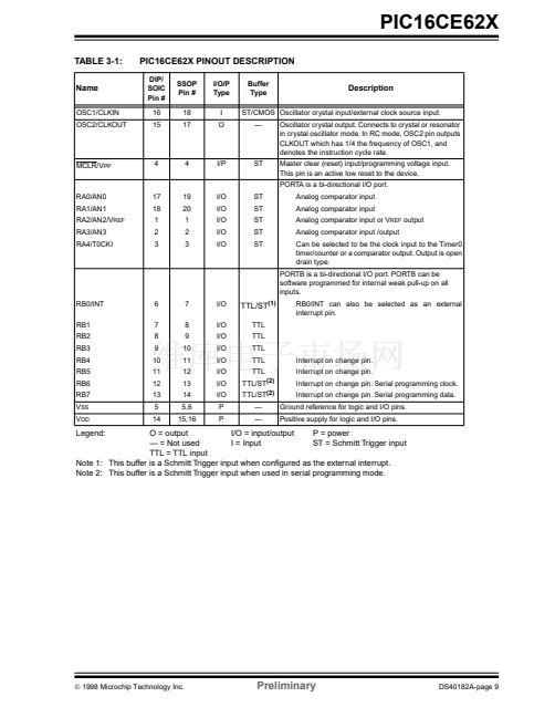
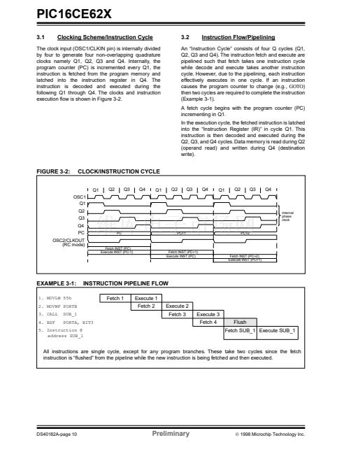
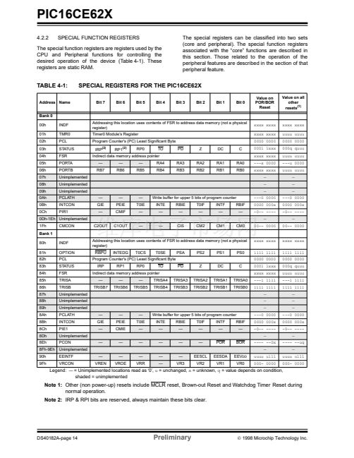
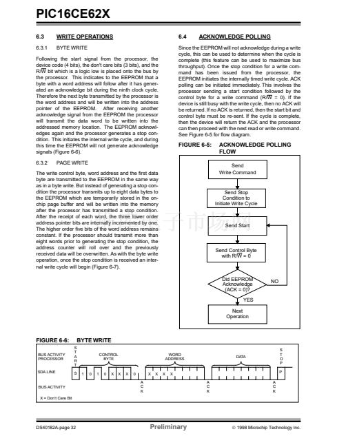
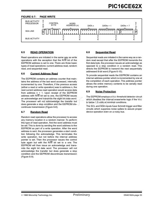
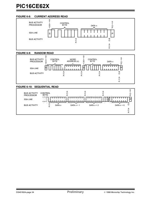
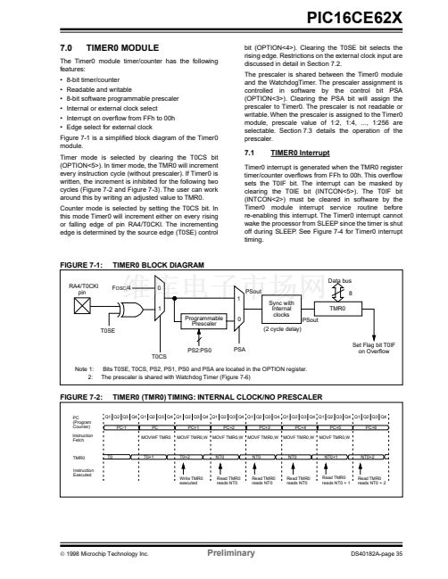
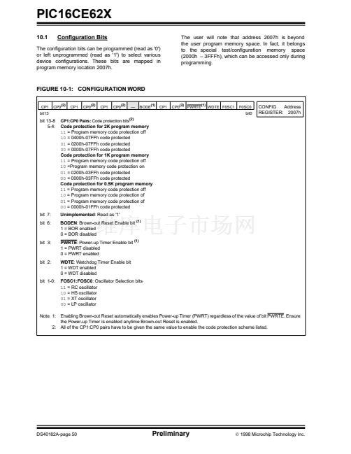
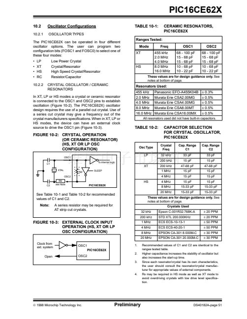
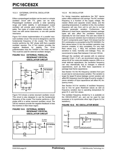
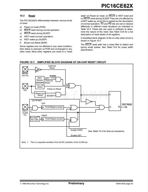
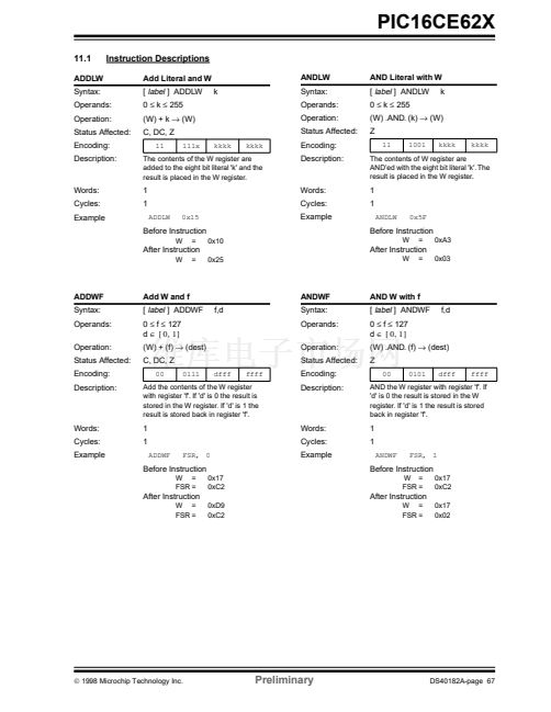
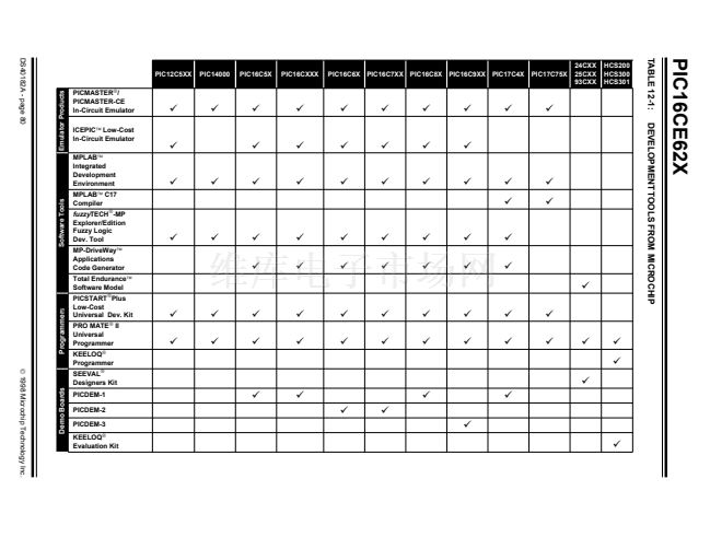
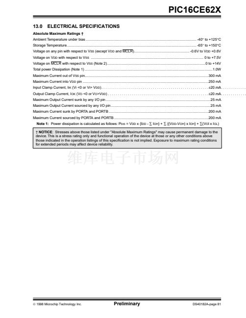
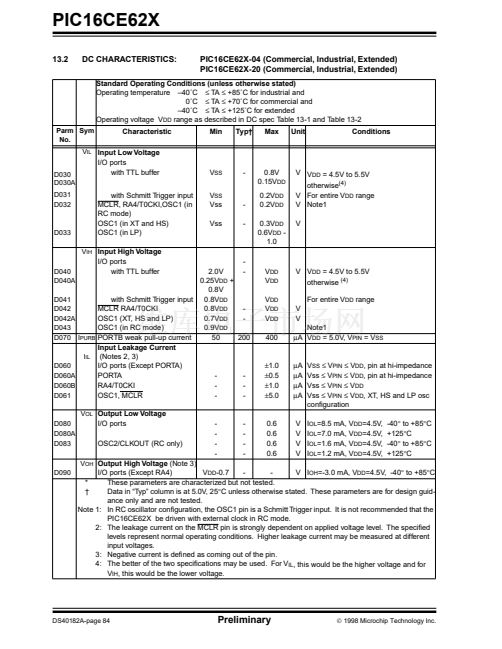
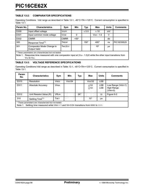
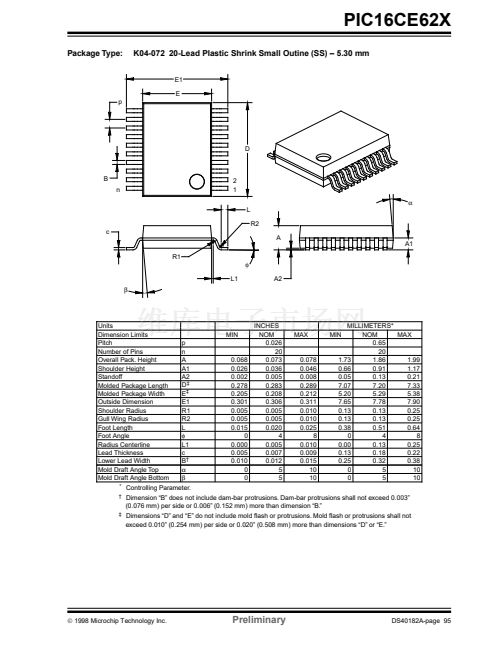
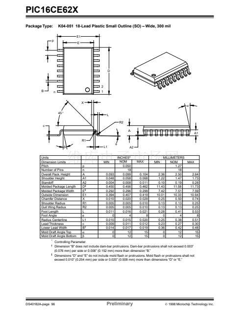
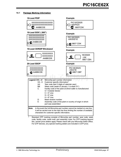
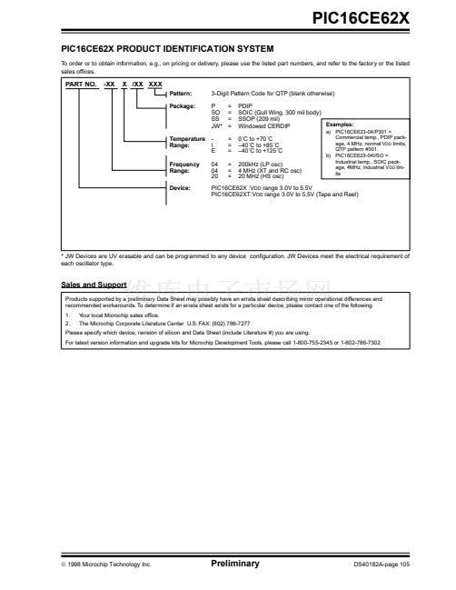
PIC16CE62X
5.0
I/O PORTS
Note:
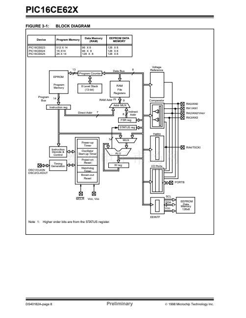
The PIC16CE62X parts have two ports, PORTA and
PORTB. Some pins for these I/O ports are multiplexed
with an alternate function for the peripheral features on
the device. In general, when a peripheral is enabled,
that pin may not be used as a general purpose I/O pin.
On reset, the TRISA register is set to all
inputs. The digital inputs are disabled and
the comparator inputs are forced to ground
to reduce excess current consumption.
5.1
PORTA and TRISA Registers
TRISA controls the direction of the RA pins, even when
they are being used as comparator inputs. The user
must make sure to keep the pins con铿乬ured as inputs
when using them as comparator inputs.
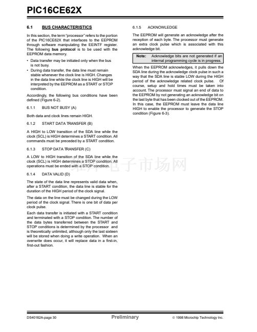
The RA2 pin will also function as the output for the
voltage reference. When in this mode, the V
REF
pin is a
very high impedance output. The user must con铿乬ure
TRISA<2> bit as an input and use high impedance
loads.
In one of the comparator modes de铿乶ed by the
CMCON register, pins RA3 and RA4 become outputs
of the comparators. The TRISA<4:3> bits must be
cleared to enable outputs to use this function.
PORTA is a 5-bit wide latch. RA4 is a Schmitt Trigger input
and an open drain output. Port RA4 is multiplexed with the
T0CKI clock input. All other RA port pins have Schmitt
Trigger input levels and full CMOS output drivers. All pins
have data direction bits (TRIS registers) which can con铿乬-
ure these pins as input or output.
A '1' in the TRISA register puts the corresponding output
driver in a hi- impedance mode. A '0' in the TRISA register
puts the contents of the output latch on the selected pin(s).
Reading the PORTA register reads the status of the pins
whereas writing to it will write to the port latch. All write
operations are read-modify-write operations. So a write
to a port implies that the port pins are 铿乺st read, then this
value is modi铿乪d and written to the port data latch.
The PORTA pins are multiplexed with comparator and
voltage reference functions. The operation of these
pins are selected by control bits in the CMCON
(comparator control register) register and the VRCON
(voltage reference control register) register. When
selected as a comparator input, these pins will read
as '0's.
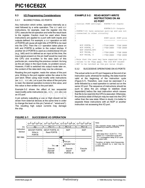
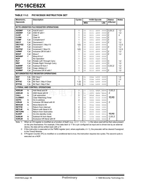
EXAMPLE 5-1:
CLRF
PORTA
INITIALIZING PORTA
;Initialize PORTA by setting
;output data latches
MOVLW 0X07
;Turn comparators off and
MOVWF CMCON
;enable pins for I/O
;functions
BSF
STATUS, RP0 ;Select Bank1
MOVLW 0x1F
;Value used to initialize
;data direction
MOVWF TRISA
;Set RA<4:0> as inputs
;TRISA<7:5> are always
;read as '0'.
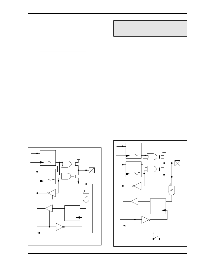
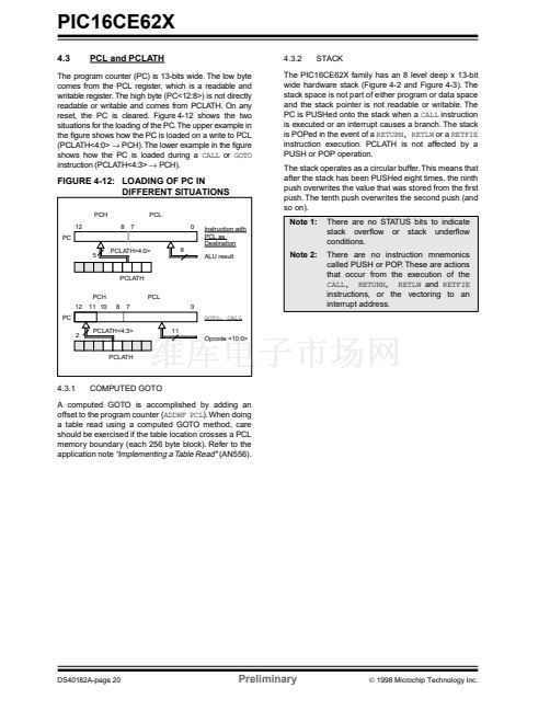
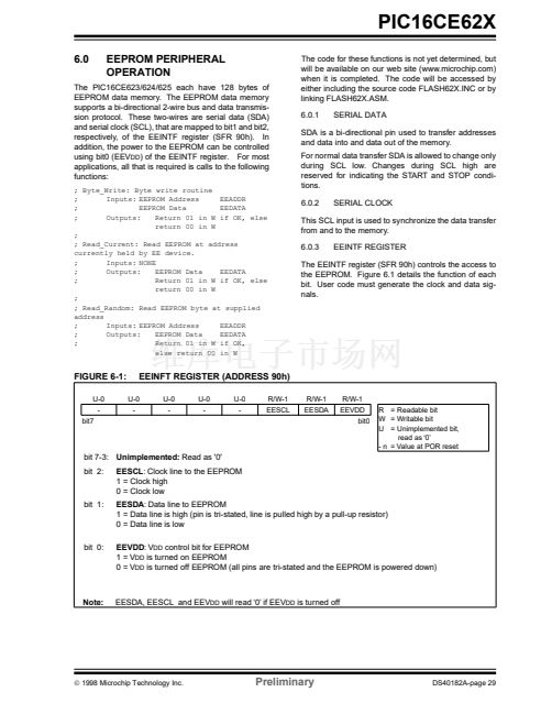
FIGURE 5-1:
Data
bus
WR
PortA
BLOCK DIAGRAM OF
RA1:RA0 PINS
Q
V
DD
FIGURE 5-2:
Data
bus
WR
PortA
D
CK
D
WR
TRISA
BLOCK DIAGRAM OF RA2 PIN
Q
V
DD
Q
Q
N
RA2 Pin
Q
V
SS
Analog
Input Mode
Schmitt Trigger
Input Buffer
Q
EN
D
P
D
CK
D
Data Latch
Q
Q
P
Data Latch
I/O Pin
WR
TRISA
N
CK
Q
V
SS
Analog
Input Mode
TRIS Latch
CK
TRIS Latch
RD TRISA
RD TRISA
Schmitt Trigger
Input Buffer
Q
EN
RD PORTA
D
RD PORTA
To Comparator
V
ROE
V
REF
Note: I/O pins have protection diodes to V
DD
and V
SS
.
To Comparator
Note: I/O pins have protection diodes to V
DD
and V
SS
.
漏
1998 Microchip Technology Inc.
Preliminary
DS40182A-page 23


 1
1
 2
2
 3
3
 4
4
 5
5
 6
6
 7
7
 8
8
 9
9
 10
10
 11
11
 12
12
 13
13
 14
14
 15
15
 16
16
 17
17
 18
18
 19
19
 20
20
 21
21
 22
22
 23
23
 24
24
 25
25
 26
26
 27
27
 28
28
 29
29
 30
30
 31
31
 32
32
 33
33
 34
34
 35
35
 36
36
 37
37
 38
38
 39
39
 40
40
 41
41
 42
42
 43
43
 44
44
 45
45
 46
46
 47
47
 48
48
 49
49
 50
50
 51
51
 52
52
 53
53
 54
54
 55
55
 56
56
 57
57
 58
58
 59
59
 60
60
 61
61
 62
62
 63
63
 64
64
 65
65
 66
66
 67
67
 68
68
 69
69
 70
70
 71
71
 72
72
 73
73
 74
74
 75
75
 76
76
 77
77
 78
78
 79
79
 80
80
 81
81
 82
82
 83
83
 84
84
 85
85
 86
86
 87
87
 88
88
 89
89
 90
90
 91
91
 92
92
 93
93
 94
94
 95
95
 96
96
 97
97
 98
98
 99
99
 100
100
 101
101
 102
102
 103
103
 104
104
 105
105
 106
106
 107
107
 108
108
