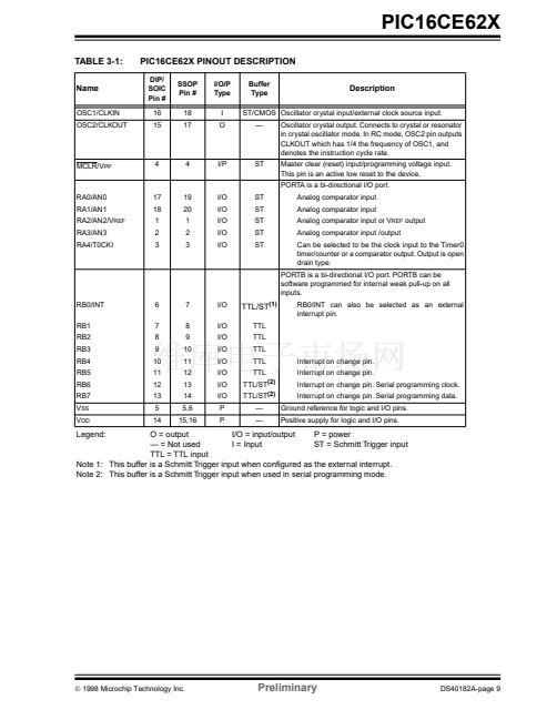
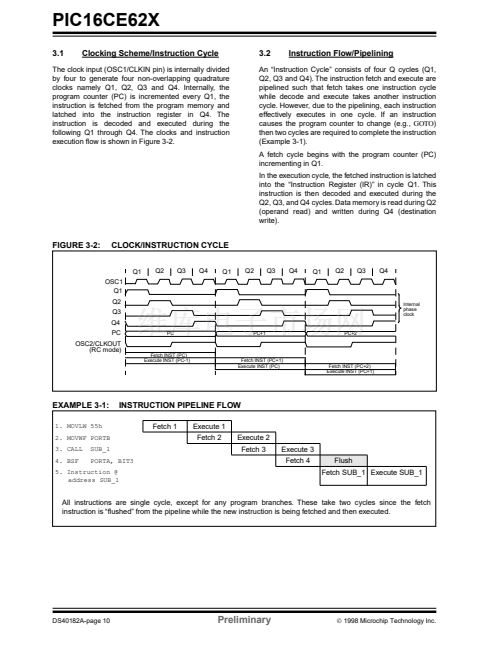
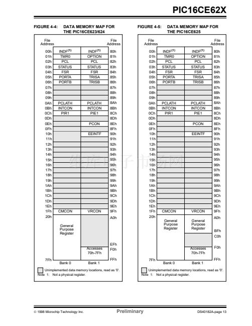
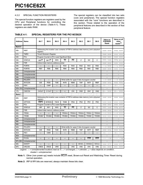
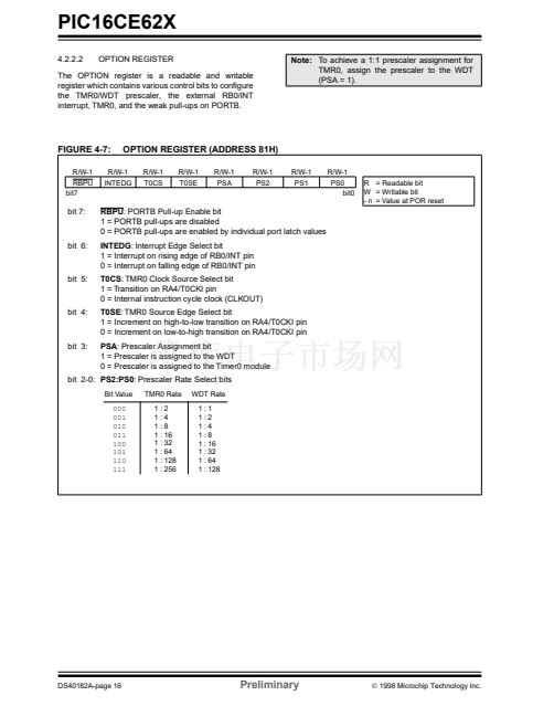
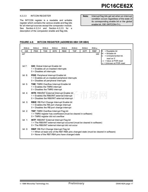
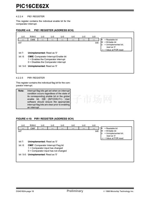
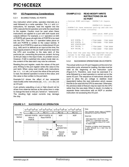
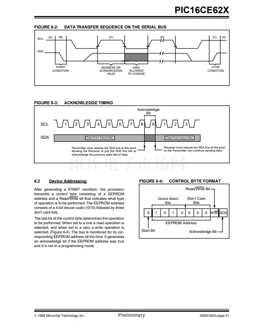
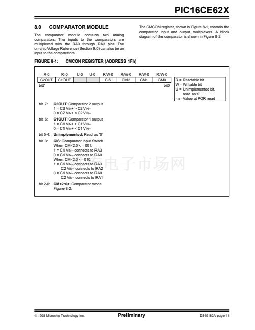
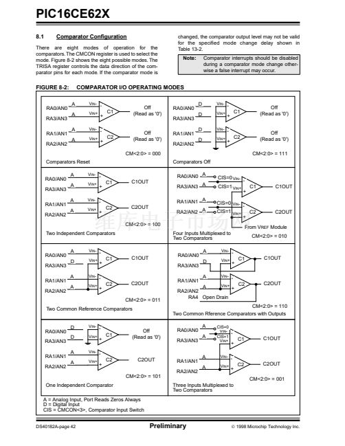
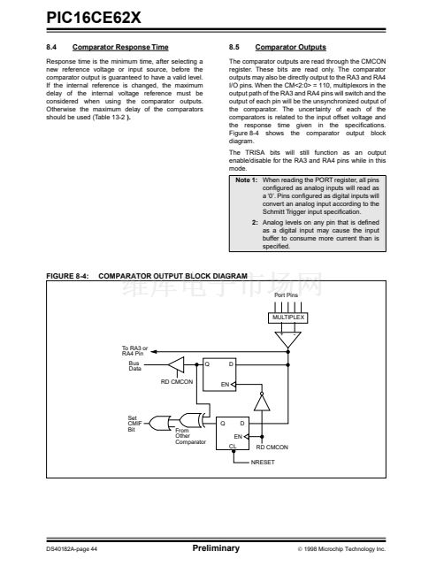
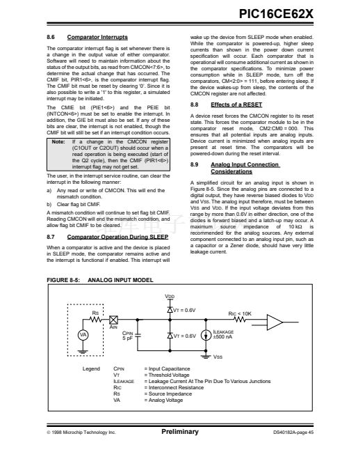
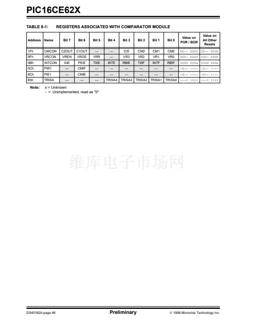
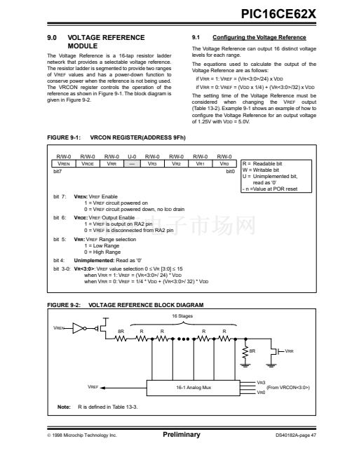
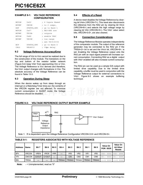
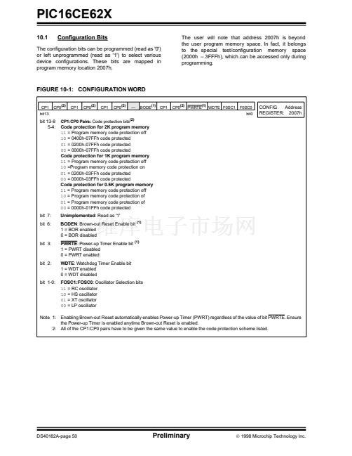
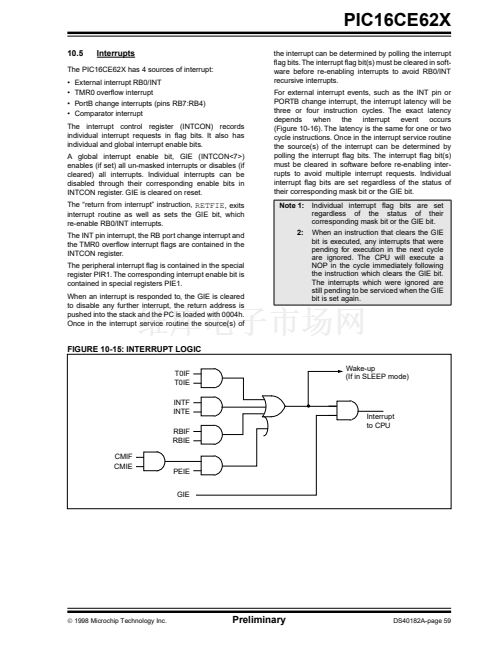
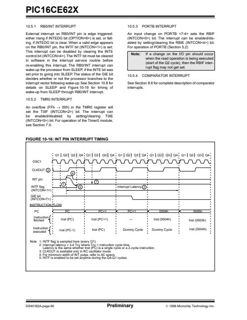
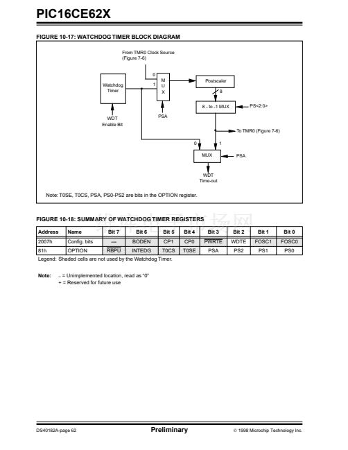
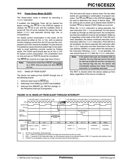
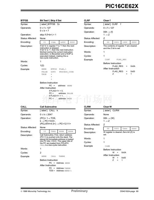
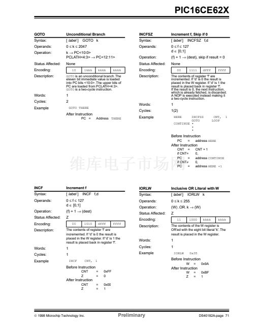
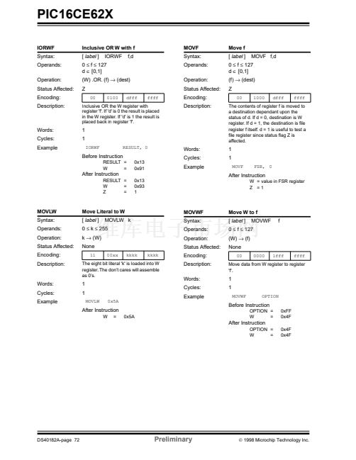
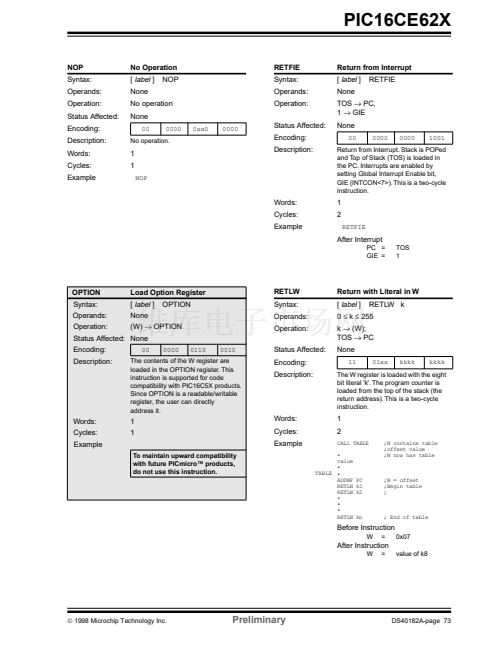
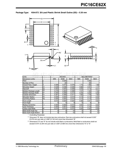
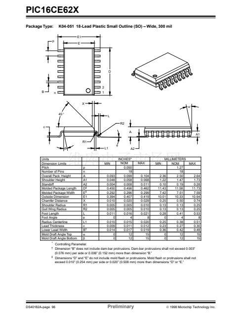
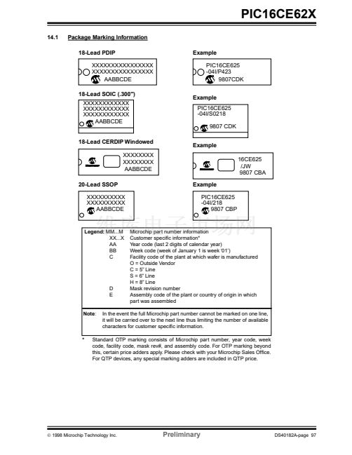
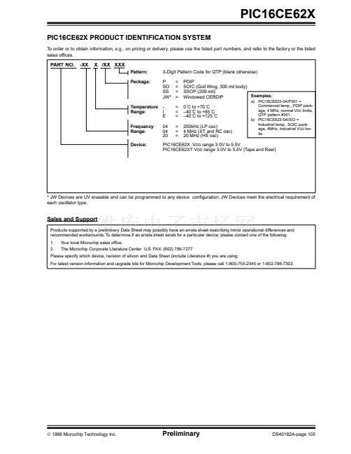
PIC16CE62X
6.0
EEPROM PERIPHERAL
OPERATION
The code for these functions is not yet determined, but
will be available on our web site (www.microchip.com)
when it is completed. The code will be accessed by
either including the source code FLASH62X.INC or by
linking FLASH62X.ASM.
6.0.1
SERIAL DATA
The PIC16CE623/624/625 each have 128 bytes of
EEPROM data memory. The EEPROM data memory
supports a bi-directional 2-wire bus and data transmis-
sion protocol. These two-wires are serial data (SDA)
and serial clock (SCL), that are mapped to bit1 and bit2,
respectively, of the EEINTF register (SFR 90h). In
addition, the power to the EEPROM can be controlled
using bit0 (EEV
DD
) of the EEINTF register. For most
applications, all that is required is calls to the following
functions:
; Byte_Write: Byte write routine
;
Inputs: EEPROM Address
EEADDR
;
EEPROM Data
EEDATA
;
Outputs:
Return 01 in W if OK, else
return 00 in W
;
; Read_Current: Read EEPROM at address
currently held by EE device.
;
Inputs: NONE
;
Outputs:
EEPROM Data
EEDATA
;
Return 01 in W if OK, else
return 00 in W
;
; Read_Random: Read EEPROM byte at supplied
address
;
Inputs: EEPROM Address
EEADDR
;
Outputs:
EEPROM Data
EEDATA
;
Return 01 in W if OK,
else return 00 in W
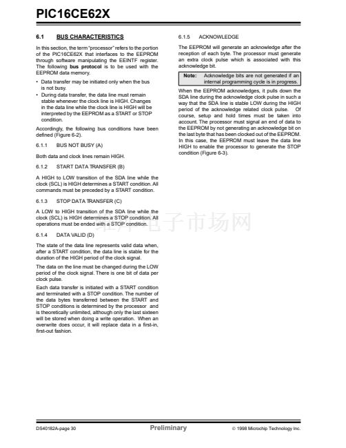
SDA is a bi-directional pin used to transfer addresses
and data into and data out of the memory.
For normal data transfer SDA is allowed to change only
during SCL low. Changes during SCL high are
reserved for indicating the START and STOP condi-
tions.
6.0.2
SERIAL CLOCK
This SCL input is used to synchronize the data transfer
from and to the memory.
6.0.3
EEINTF REGISTER
The EEINTF register (SFR 90h) controls the access to
the EEPROM. Figure 6.1 details the function of each
bit. User code must generate the clock and data sig-
nals.
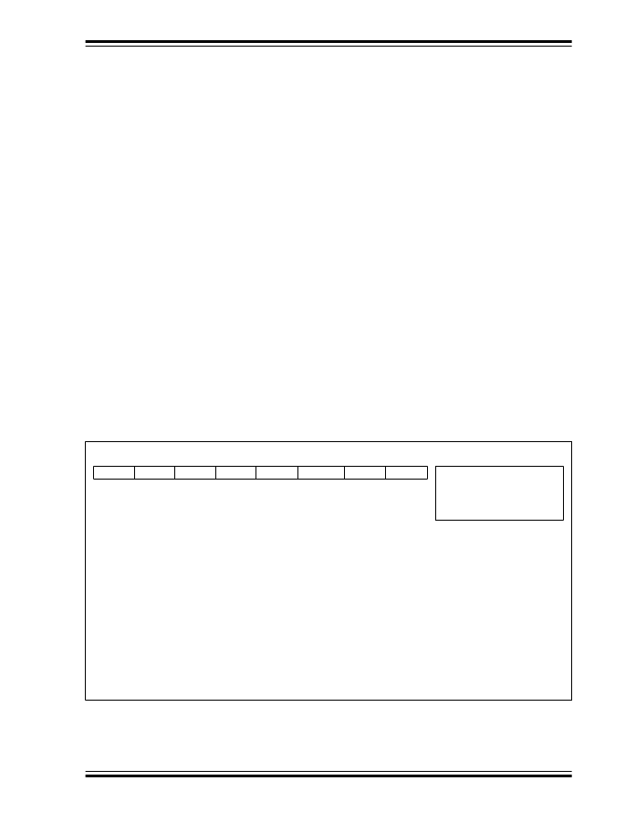
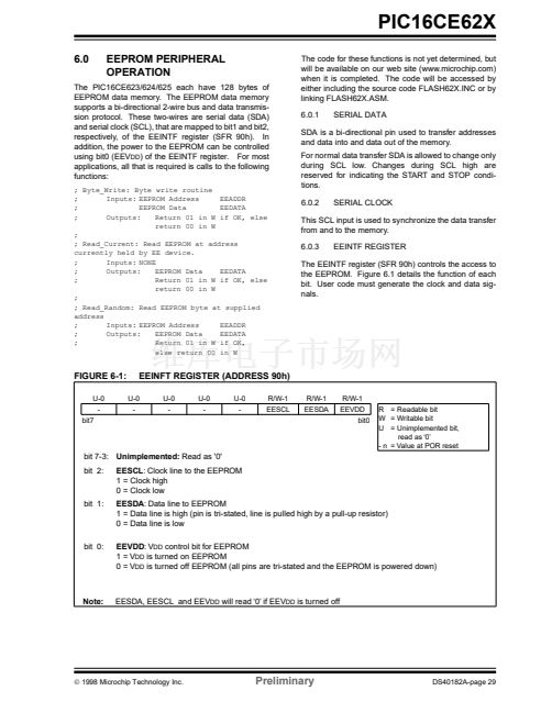
FIGURE 6-1:
U-0
-
bit7
EEINFT REGISTER (ADDRESS 90h)
U-0
-
U-0
-
U-0
-
U-0
-
R/W-1
EESCL
R/W-1
EESDA
R/W-1
EEVDD
bit0
R = Readable bit
W = Writable bit
U = Unimplemented bit,
read as 鈥?鈥?/div>
- n = Value at POR reset
bit 7-3:
Unimplemented:
Read as '0'
bit 2:
EESCL:
Clock line to the EEPROM
1 = Clock high
0 = Clock low
EESDA:
Data line to EEPROM
1 = Data line is high (pin is tri-stated, line is pulled high by a pull-up resistor)
0 = Data line is low
EEVDD:
V
DD
control bit for EEPROM
1 = V
DD
is turned on EEPROM
0 = V
DD
is turned off EEPROM (all pins are tri-stated and the EEPROM is powered down)
bit 1:
bit 0:
Note:
EESDA, EESCL and EEV
DD
will read 鈥?鈥?if EEV
DD
is turned off
漏
1998 Microchip Technology Inc.
Preliminary
DS40182A-page 29


 1
1
 2
2
 3
3
 4
4
 5
5
 6
6
 7
7
 8
8
 9
9
 10
10
 11
11
 12
12
 13
13
 14
14
 15
15
 16
16
 17
17
 18
18
 19
19
 20
20
 21
21
 22
22
 23
23
 24
24
 25
25
 26
26
 27
27
 28
28
 29
29
 30
30
 31
31
 32
32
 33
33
 34
34
 35
35
 36
36
 37
37
 38
38
 39
39
 40
40
 41
41
 42
42
 43
43
 44
44
 45
45
 46
46
 47
47
 48
48
 49
49
 50
50
 51
51
 52
52
 53
53
 54
54
 55
55
 56
56
 57
57
 58
58
 59
59
 60
60
 61
61
 62
62
 63
63
 64
64
 65
65
 66
66
 67
67
 68
68
 69
69
 70
70
 71
71
 72
72
 73
73
 74
74
 75
75
 76
76
 77
77
 78
78
 79
79
 80
80
 81
81
 82
82
 83
83
 84
84
 85
85
 86
86
 87
87
 88
88
 89
89
 90
90
 91
91
 92
92
 93
93
 94
94
 95
95
 96
96
 97
97
 98
98
 99
99
 100
100
 101
101
 102
102
 103
103
 104
104
 105
105
 106
106
 107
107
 108
108
