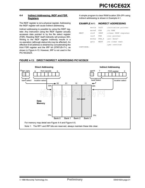
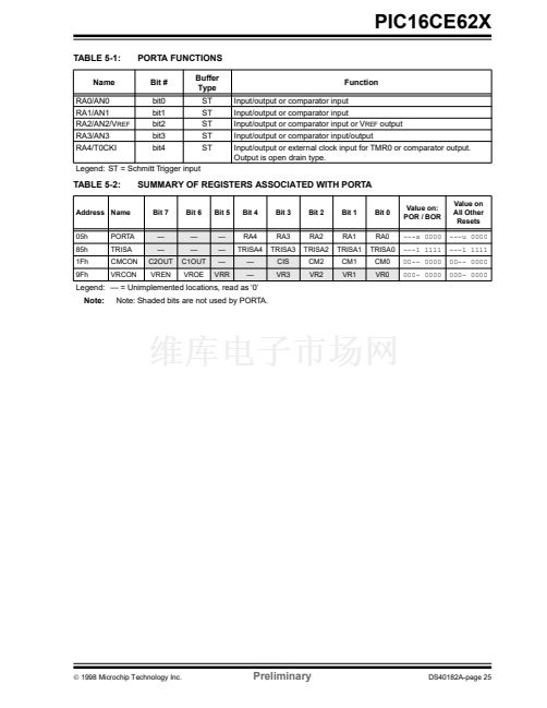
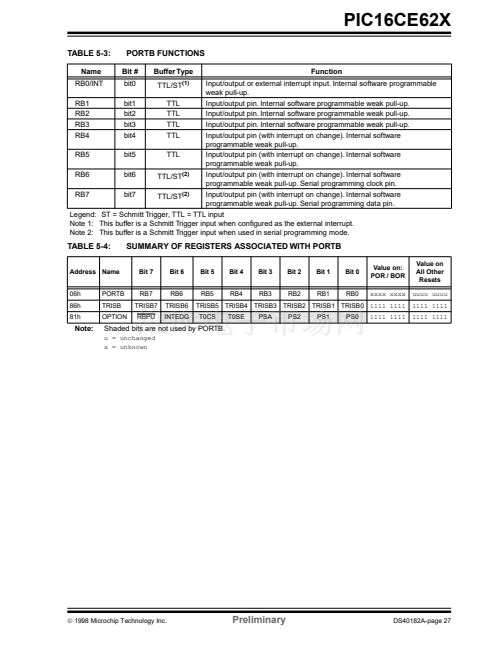
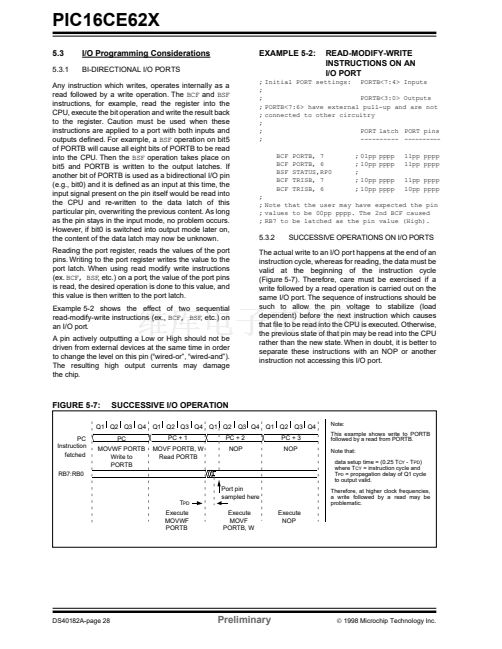
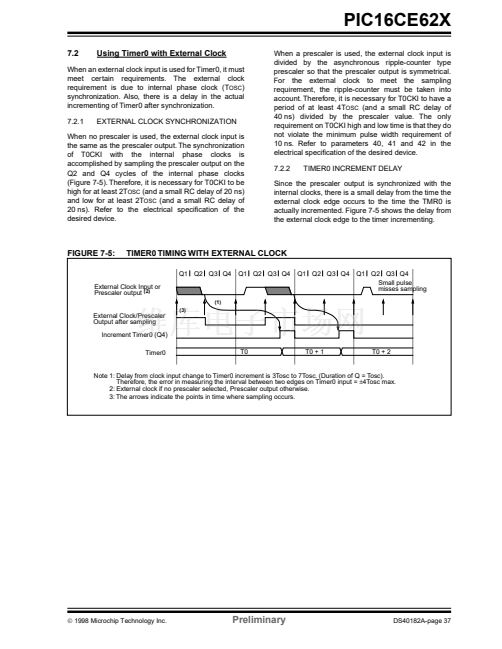
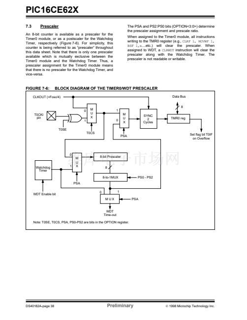
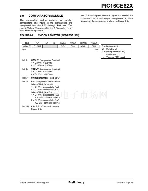
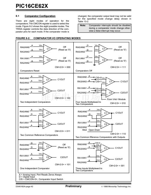
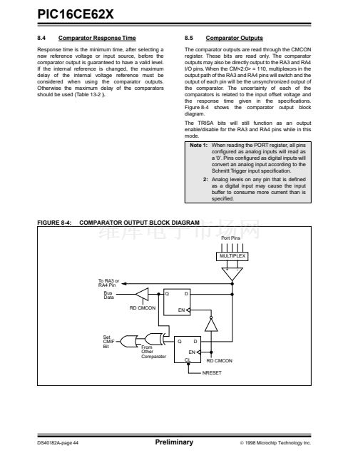
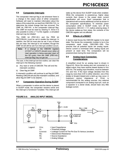
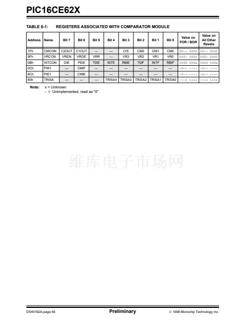
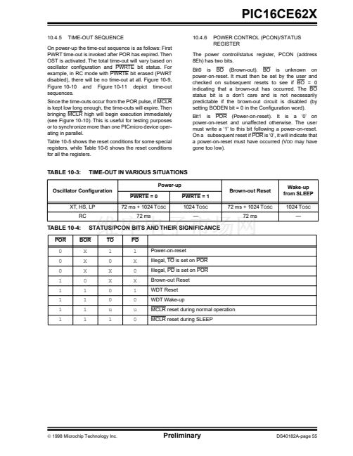
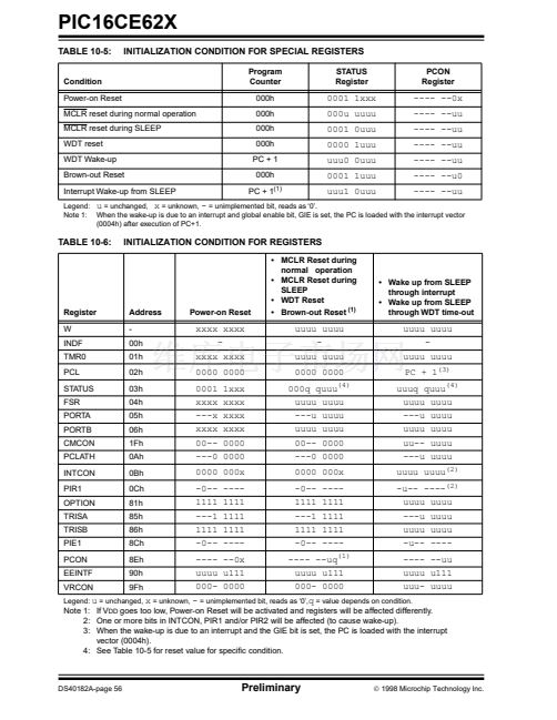
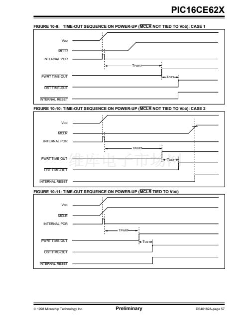
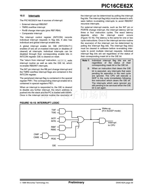
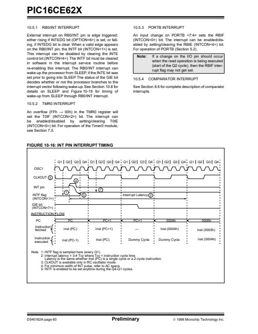
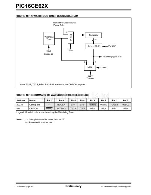
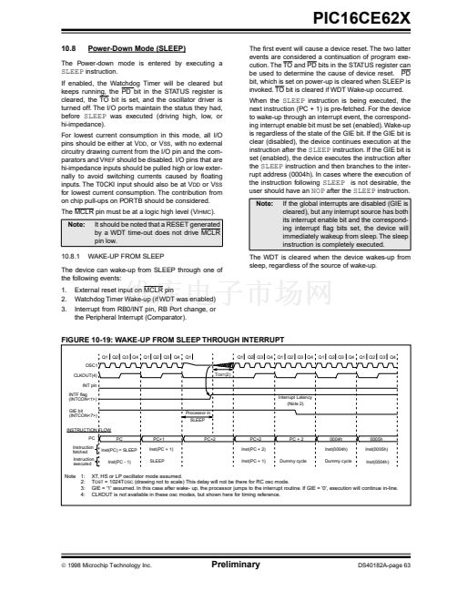
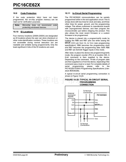
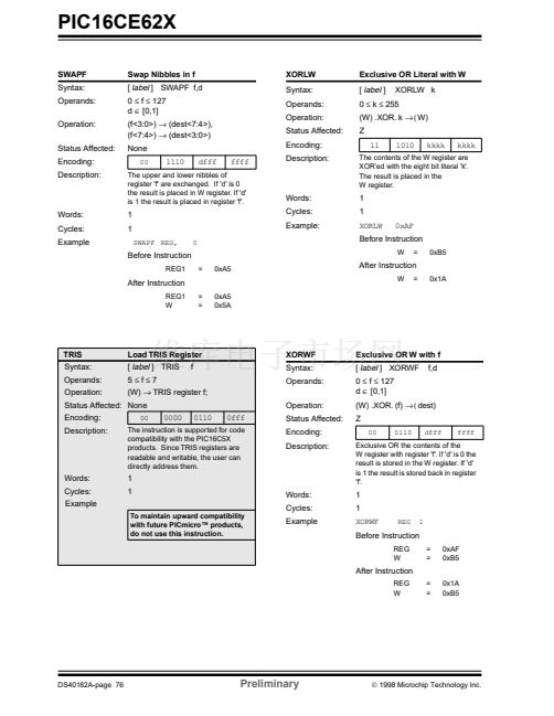
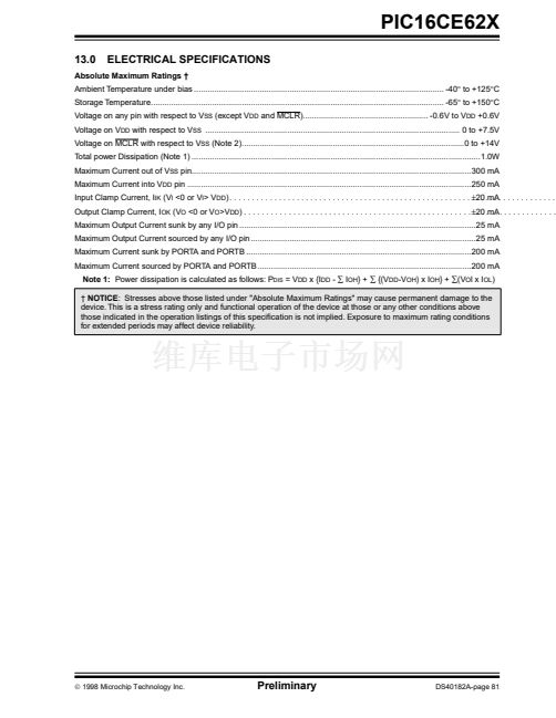
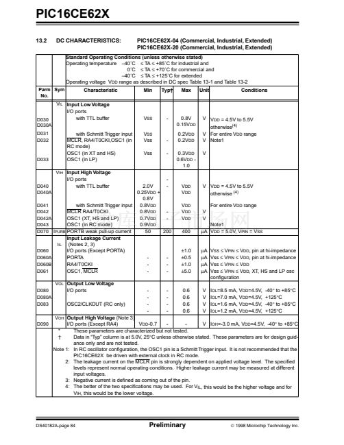
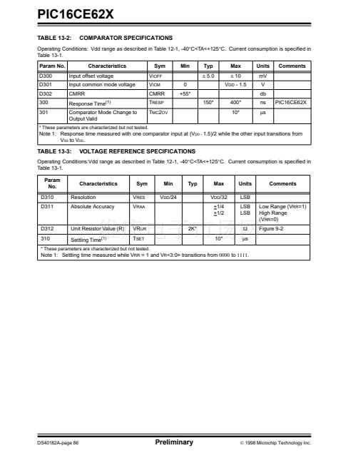
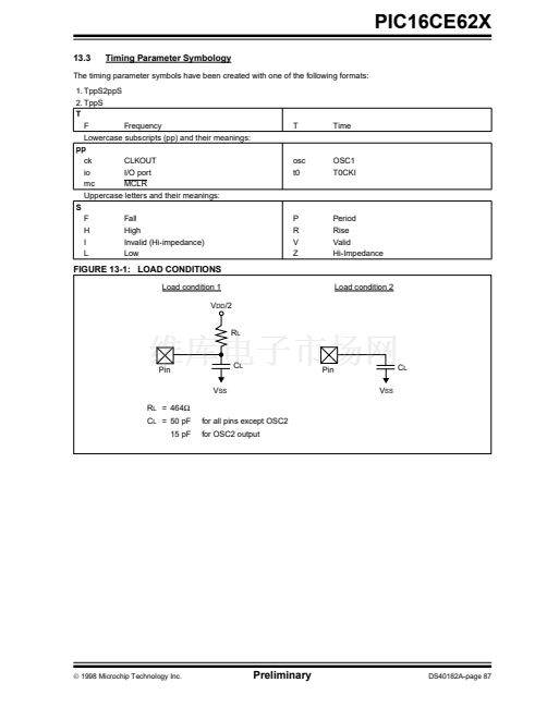
鈥?/div>
Literal and control
operations
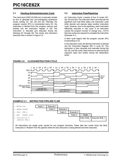
All instructions are executed within one single
instruction cycle, unless a conditional test is true or the
program counter is changed as a result of an
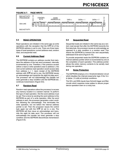
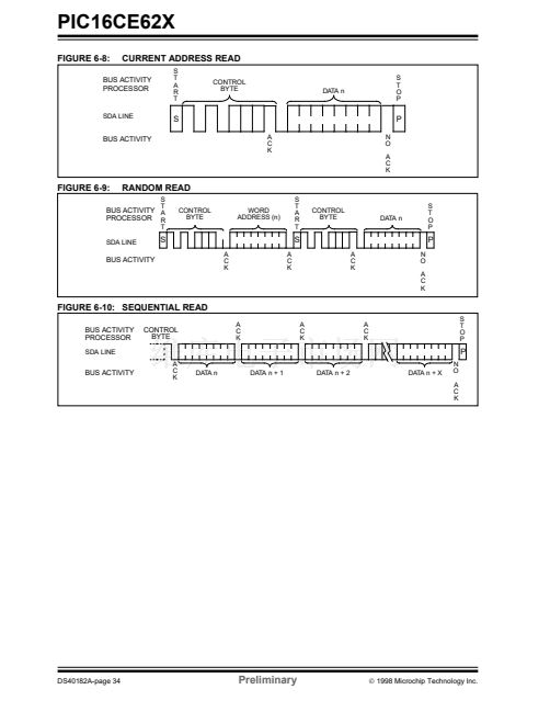
instruction. In this case, the execution takes two
instruction cycles with the second cycle executed as a
NOP. One instruction cycle consists of four oscillator
periods. Thus, for an oscillator frequency of 4 MHz, the
normal instruction execution time is 1
碌s.
If a
conditional test is true or the program counter is
changed as a result of an instruction, the instruction
execution time is 2
碌s.
Table 11-1 lists the instructions recognized by the
MPASM assembler.
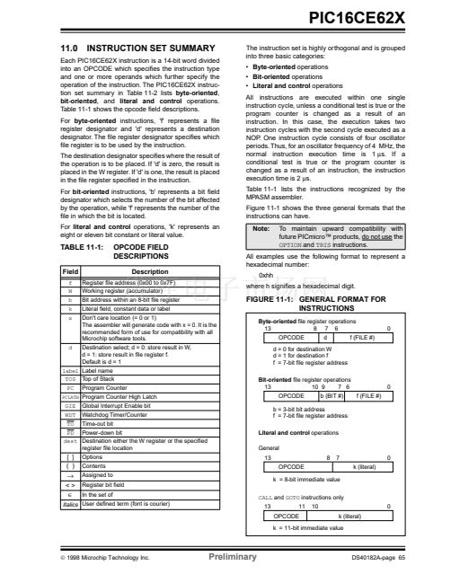
Figure 11-1 shows the three general formats that the
instructions can have.
Note:
To maintain upward compatibility with
future PICmicro鈩?products, do not use the
OPTION
and
TRIS
instructions.
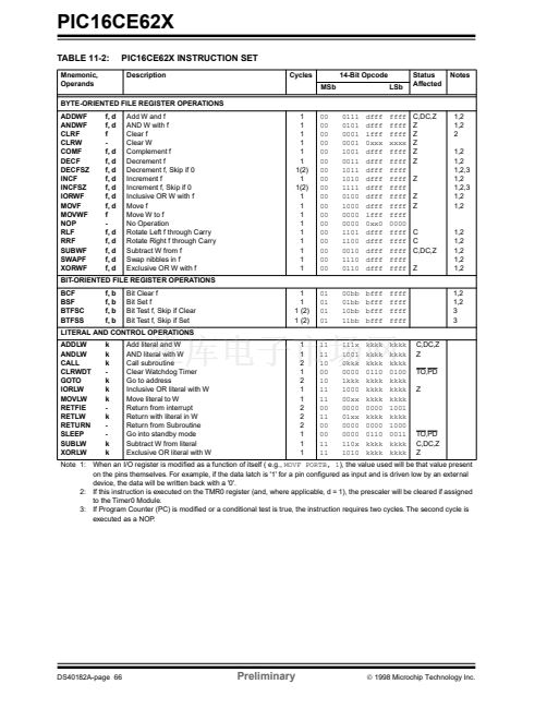
TABLE 11-1:
Field
f
W
b
k
x
OPCODE FIELD
DESCRIPTIONS
Description
All examples use the following format to represent a
hexadecimal number:
0xhh
where h signi铿乪s a hexadecimal digit.
Register 铿乴e address (0x00 to 0x7F)
Working register (accumulator)
Bit address within an 8-bit 铿乴e register
Literal 铿乪ld, constant data or label
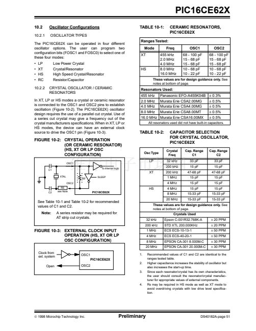
FIGURE 11-1: GENERAL FORMAT FOR
INSTRUCTIONS
Byte-oriented
铿乴e register operations
13
8 7 6
OPCODE
d
f (FILE #)
d = 0 for destination W
d = 1 for destination f
f = 7-bit 铿乴e register address
Bit-oriented
铿乴e register operations
13
10 9
7 6
OPCODE
b (BIT #)
f (FILE #)
b = 3-bit bit address
f = 7-bit 铿乴e register address
Literal and control
operations
General
13
OPCODE
k = 8-bit immediate value
CALL
and
GOTO
instructions only
13
11
OPCODE
10
k (literal)
0
8
7
k (literal)
0
0
Don't care location (= 0 or 1)
The assembler will generate code with x = 0. It is the
recommended form of use for compatibility with all
Microchip software tools.
d
Destination select; d = 0: store result in W,
d = 1: store result in 铿乴e register f.
Default is d = 1
label
Label name
TOS
PC
GIE
WDT
TO
PD
dest
[ ]
Top of Stack
Program Counter
Global Interrupt Enable bit
Watchdog Timer/Counter
Time-out bit
Power-down bit
Destination either the W register or the speci铿乪d
register 铿乴e location
Options
Contents
Assigned to
Register bit 铿乪ld
In the set of
0
PCLATH
Program Counter High Latch
( )
鈫?/div>
<>
鈭?/div>
i
talics
User de铿乶ed term (font is courier)
k = 11-bit immediate value
漏
1998 Microchip Technology Inc.
Preliminary
DS40182A-page 65


 1
1
 2
2
 3
3
 4
4
 5
5
 6
6
 7
7
 8
8
 9
9
 10
10
 11
11
 12
12
 13
13
 14
14
 15
15
 16
16
 17
17
 18
18
 19
19
 20
20
 21
21
 22
22
 23
23
 24
24
 25
25
 26
26
 27
27
 28
28
 29
29
 30
30
 31
31
 32
32
 33
33
 34
34
 35
35
 36
36
 37
37
 38
38
 39
39
 40
40
 41
41
 42
42
 43
43
 44
44
 45
45
 46
46
 47
47
 48
48
 49
49
 50
50
 51
51
 52
52
 53
53
 54
54
 55
55
 56
56
 57
57
 58
58
 59
59
 60
60
 61
61
 62
62
 63
63
 64
64
 65
65
 66
66
 67
67
 68
68
 69
69
 70
70
 71
71
 72
72
 73
73
 74
74
 75
75
 76
76
 77
77
 78
78
 79
79
 80
80
 81
81
 82
82
 83
83
 84
84
 85
85
 86
86
 87
87
 88
88
 89
89
 90
90
 91
91
 92
92
 93
93
 94
94
 95
95
 96
96
 97
97
 98
98
 99
99
 100
100
 101
101
 102
102
 103
103
 104
104
 105
105
 106
106
 107
107
 108
108
