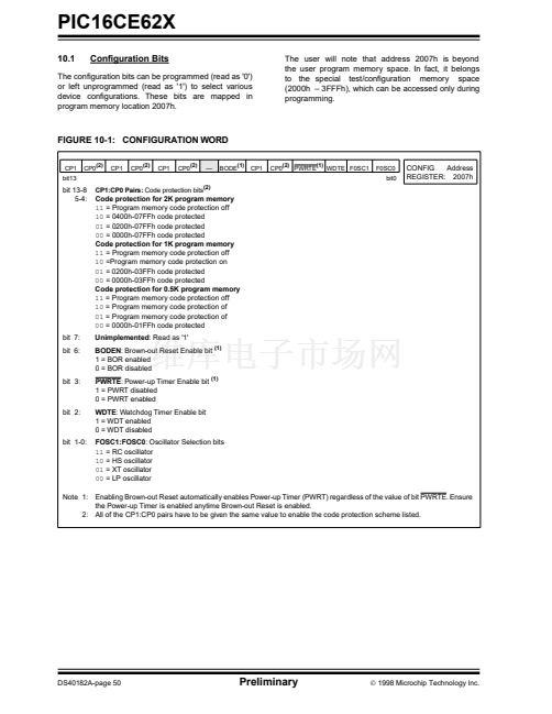
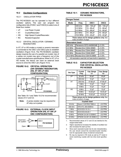
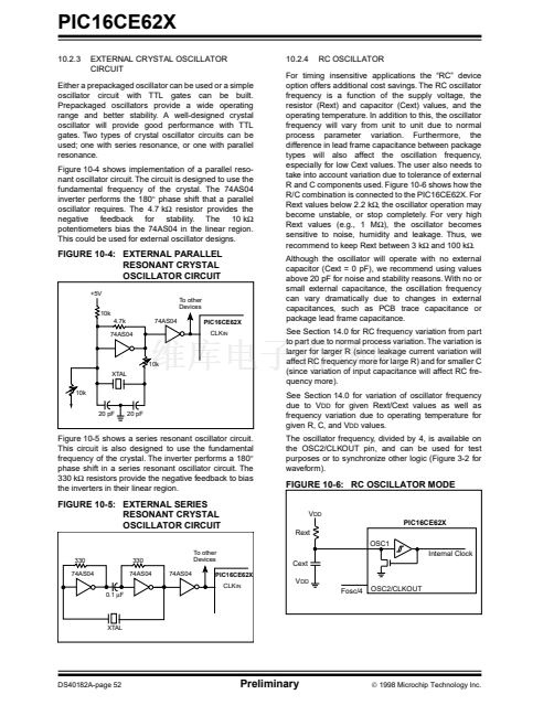
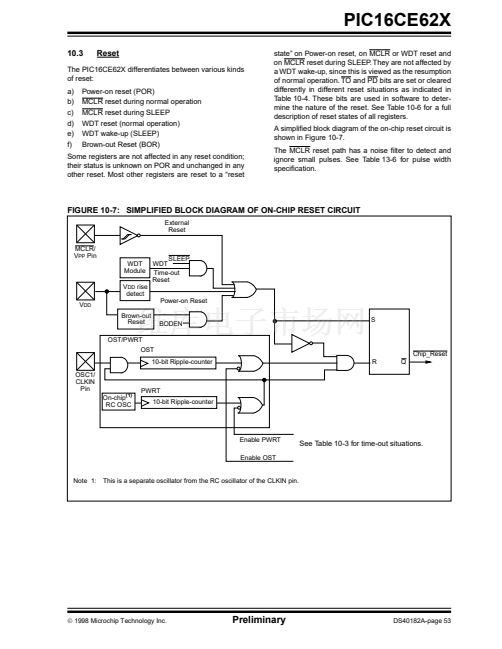
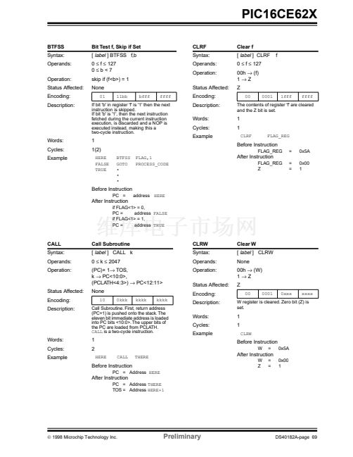
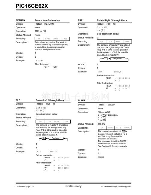
IN鈥?/div>
V
IN+
Output
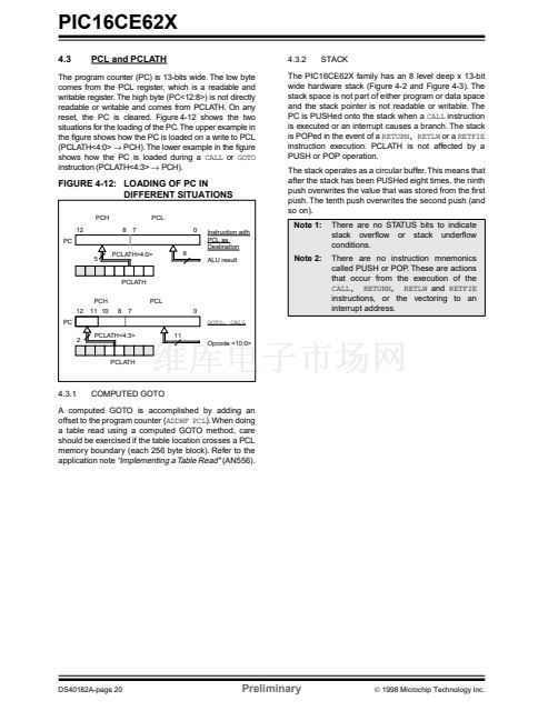
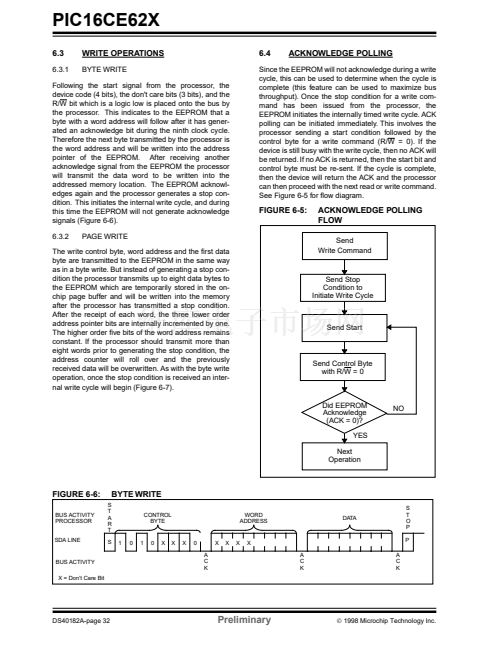
8.2
Comparator Operation
8.3.1
EXTERNAL REFERENCE SIGNAL
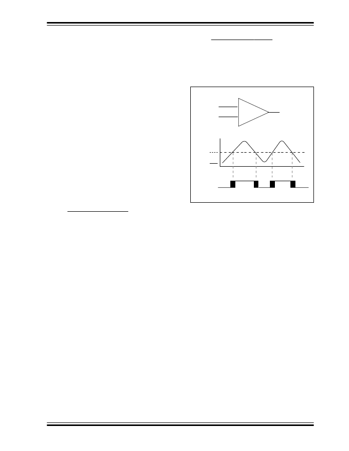
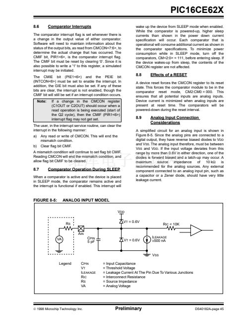
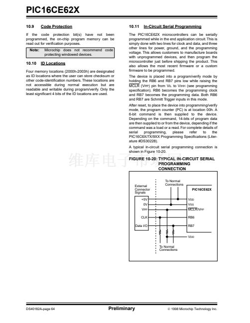
A single comparator is shown in Figure 8-3 along with
the relationship between the analog input levels and
the digital output. When the analog input at V
IN
+ is less
than the analog input V
IN
鈥? the output of the
comparator is a digital low level. When the analog input
at V
IN
+ is greater than the analog input V
IN
鈥? the output
of the comparator is a digital high level. The shaded
areas of the output of the comparator in Figure 8-3
represent the uncertainty due to input offsets and
response time.
When external voltage references are used, the
comparator module can be con铿乬ured to have the com-
parators operate from the same or different reference
sources. However, threshold detector applications may
require the same reference. The reference signal must
be between V
SS
and V
DD
, and can be applied to either
pin of the comparator(s).
8.3.2
INTERNAL REFERENCE SIGNAL
The comparator module also allows the selection of an
internally generated voltage reference for the
comparators. Section 13, Instruction Sets, contains a
detailed description of the Voltage Reference Module
that provides this signal. The internal reference signal
is used when the comparators are in mode
CM<2:0>=010 (Figure 8-2). In this mode, the internal
voltage reference is applied to the V
IN
+ pin of both com-
parators.
漏
1998 Microchip Technology Inc.
Preliminary
DS40182A-page 43


 1
1
 2
2
 3
3
 4
4
 5
5
 6
6
 7
7
 8
8
 9
9
 10
10
 11
11
 12
12
 13
13
 14
14
 15
15
 16
16
 17
17
 18
18
 19
19
 20
20
 21
21
 22
22
 23
23
 24
24
 25
25
 26
26
 27
27
 28
28
 29
29
 30
30
 31
31
 32
32
 33
33
 34
34
 35
35
 36
36
 37
37
 38
38
 39
39
 40
40
 41
41
 42
42
 43
43
 44
44
 45
45
 46
46
 47
47
 48
48
 49
49
 50
50
 51
51
 52
52
 53
53
 54
54
 55
55
 56
56
 57
57
 58
58
 59
59
 60
60
 61
61
 62
62
 63
63
 64
64
 65
65
 66
66
 67
67
 68
68
 69
69
 70
70
 71
71
 72
72
 73
73
 74
74
 75
75
 76
76
 77
77
 78
78
 79
79
 80
80
 81
81
 82
82
 83
83
 84
84
 85
85
 86
86
 87
87
 88
88
 89
89
 90
90
 91
91
 92
92
 93
93
 94
94
 95
95
 96
96
 97
97
 98
98
 99
99
 100
100
 101
101
 102
102
 103
103
 104
104
 105
105
 106
106
 107
107
 108
108
