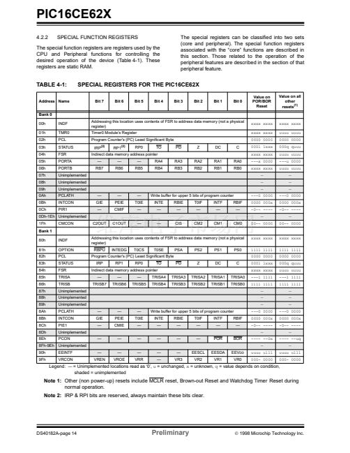
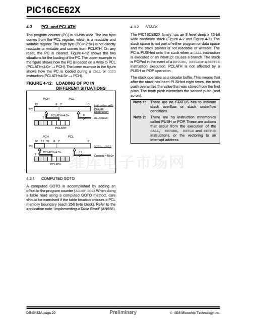
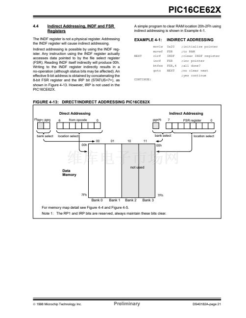
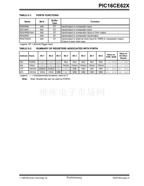
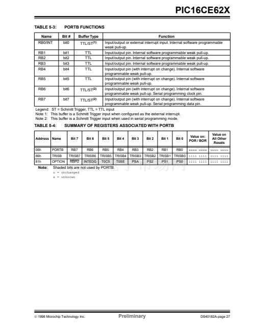
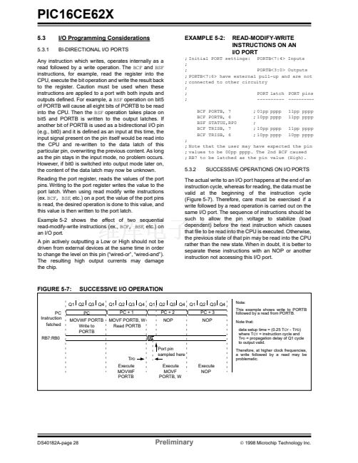
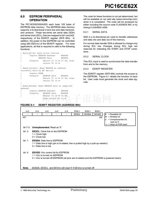
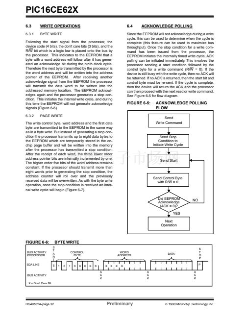
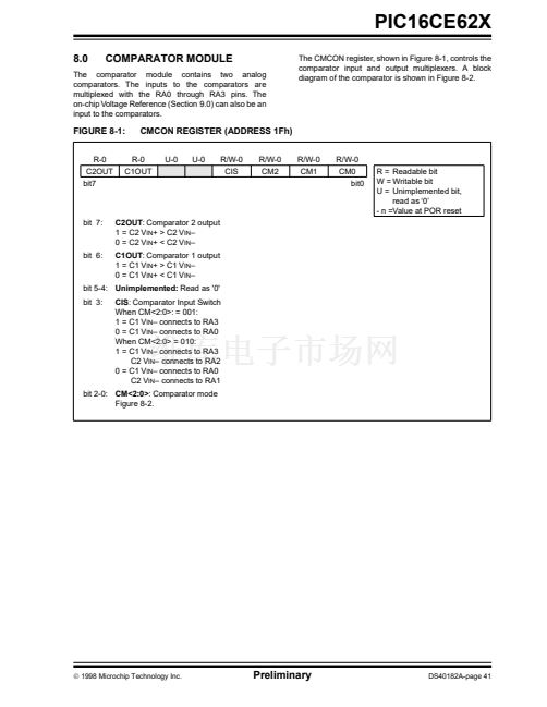
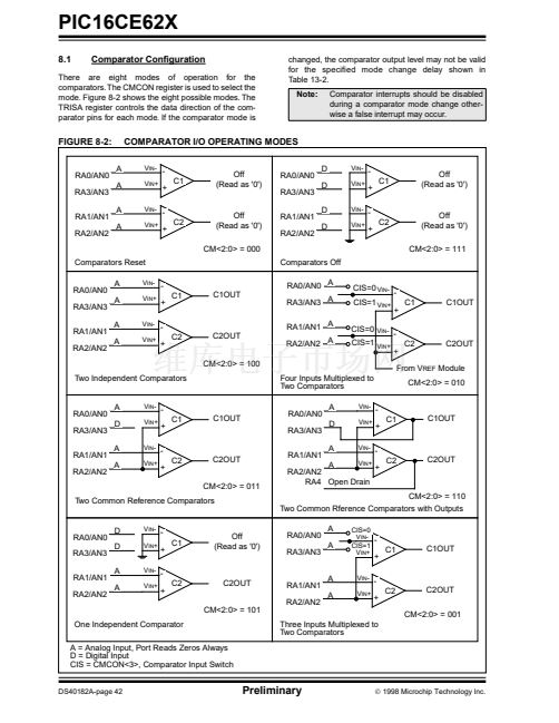
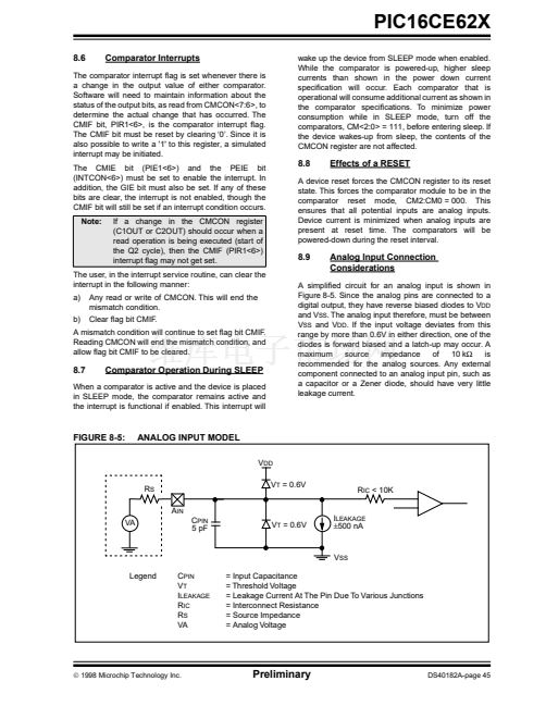
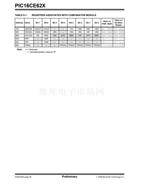
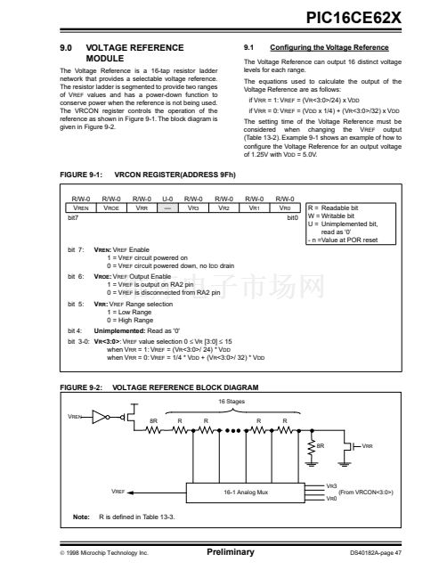
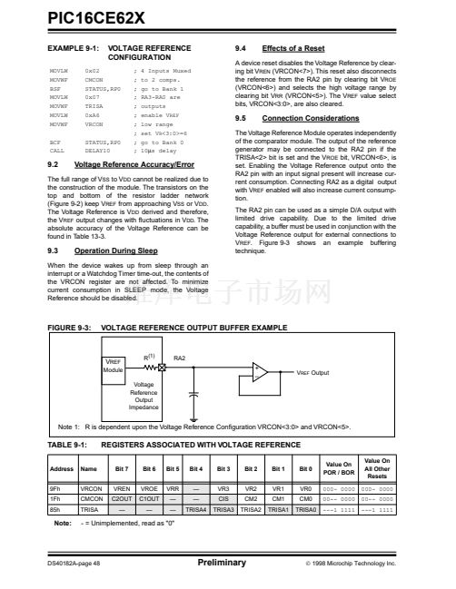
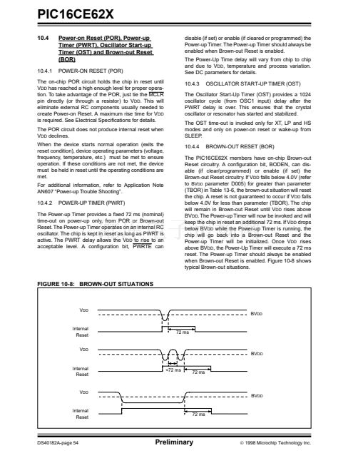
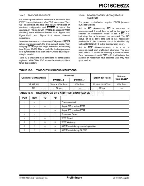
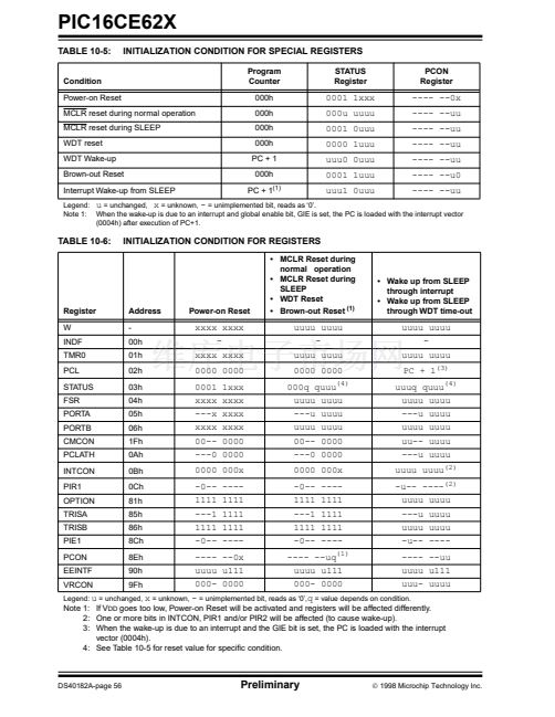
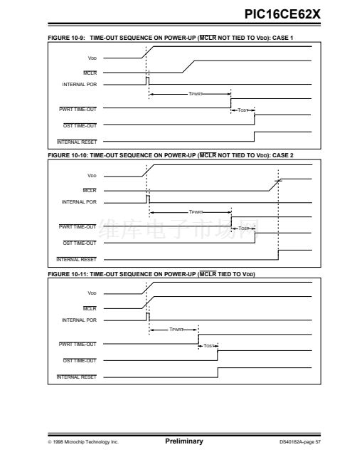
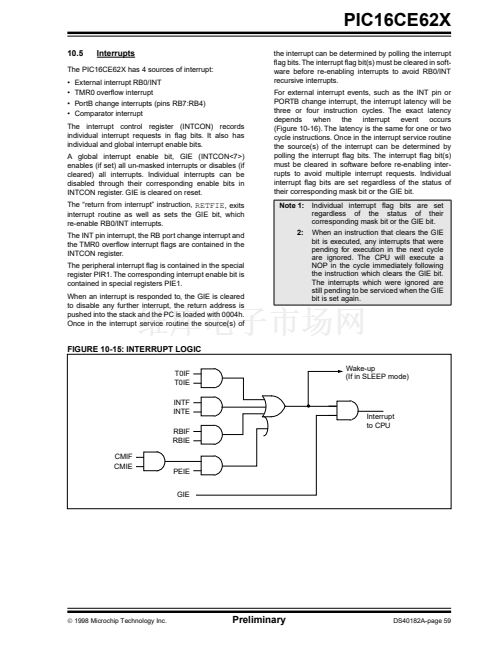
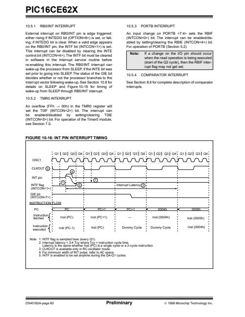
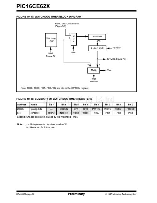
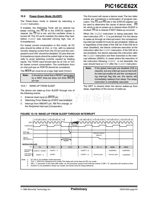
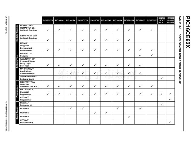
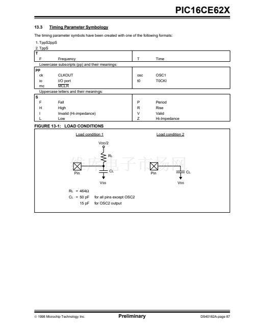
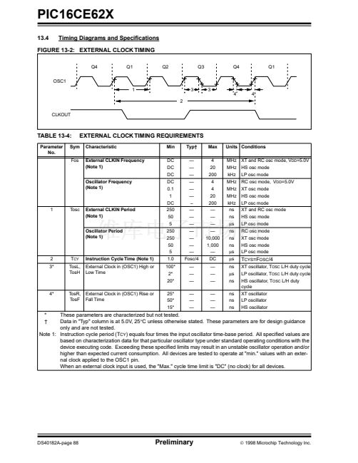
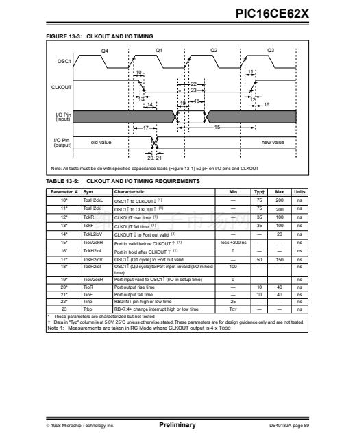
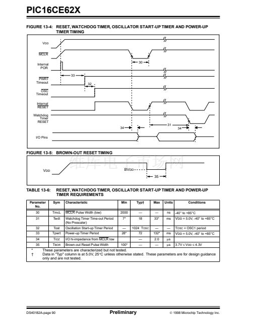
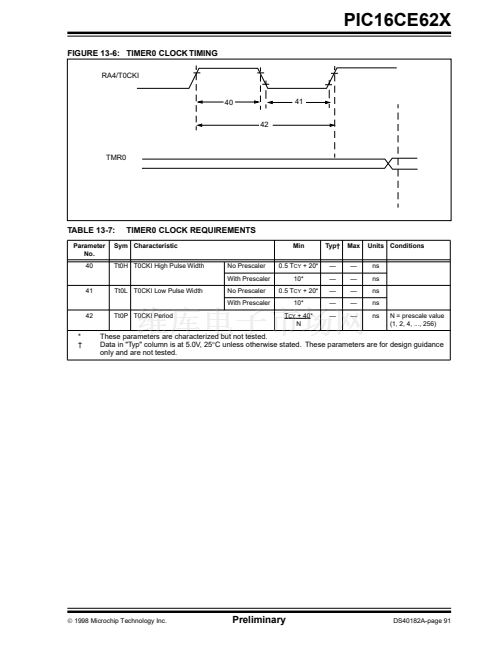
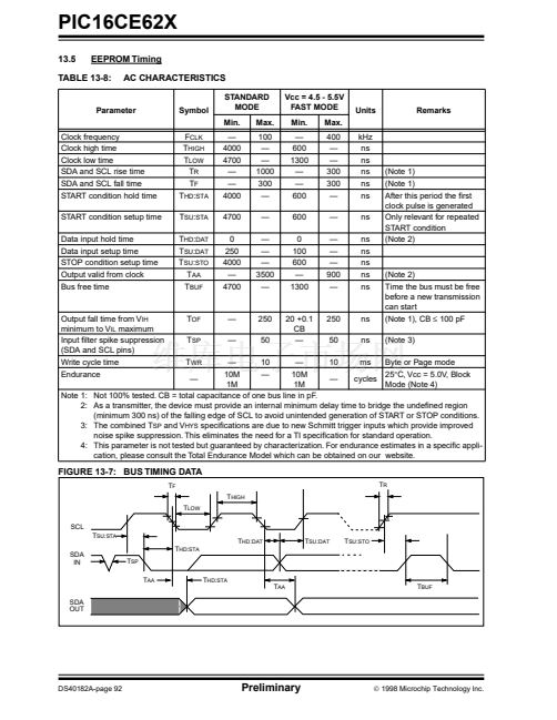
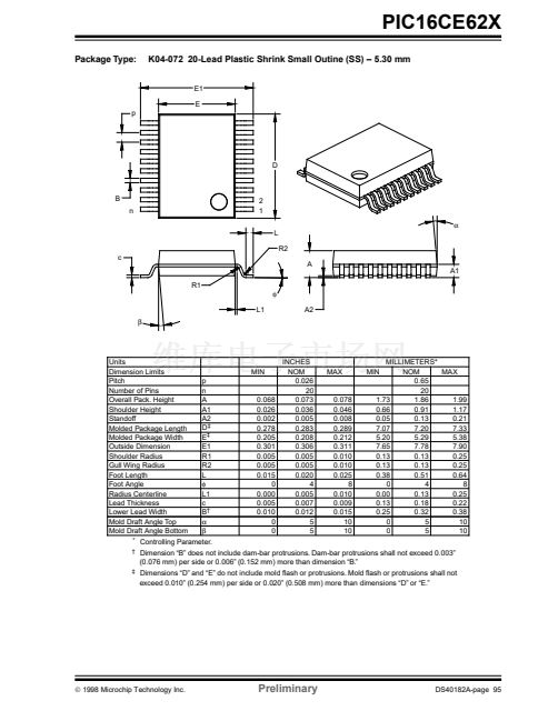
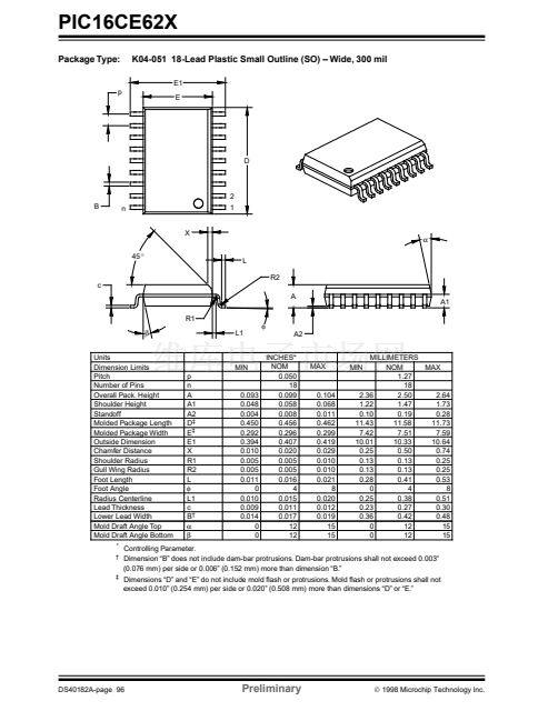
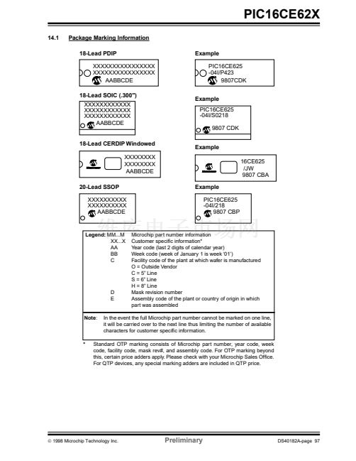
PIC16CE62X
8.4
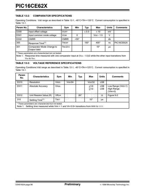
Comparator Response Time
8.5
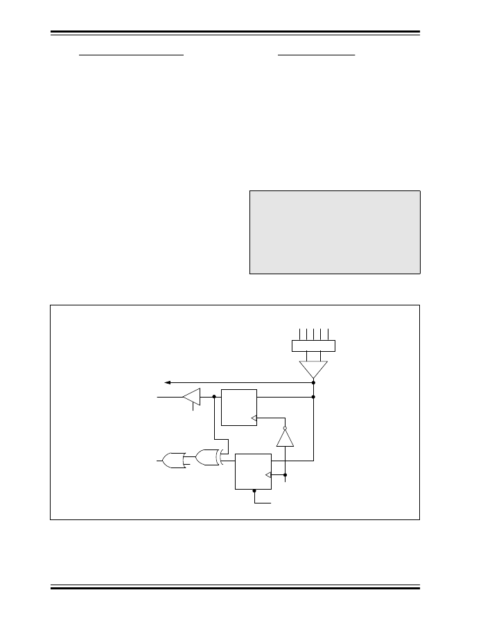
Comparator Outputs
Response time is the minimum time, after selecting a
new reference voltage or input source, before the
comparator output is guaranteed to have a valid level.
If the internal reference is changed, the maximum
delay of the internal voltage reference must be
considered when using the comparator outputs.
Otherwise the maximum delay of the comparators
should be used (Table 13-2
).
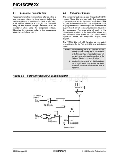
The comparator outputs are read through the CMCON
register. These bits are read only. The comparator
outputs may also be directly output to the RA3 and RA4
I/O pins. When the CM<2:0> = 110, multiplexors in the
output path of the RA3 and RA4 pins will switch and the
output of each pin will be the unsynchronized output of
the comparator. The uncertainty of each of the
comparators is related to the input offset voltage and
the response time given in the speci铿乧ations.
Figure 8-4 shows the comparator output block
diagram.
The TRISA bits will still function as an output
enable/disable for the RA3 and RA4 pins while in this
mode.
Note 1:
When reading the PORT register, all pins
con铿乬ured as analog inputs will read as
a 鈥?鈥? Pins con铿乬ured as digital inputs will
convert an analog input according to the
Schmitt Trigger input speci铿乧ation.
2:
Analog levels on any pin that is de铿乶ed
as a digital input may cause the input
buffer to consume more current than is
speci铿乪d.
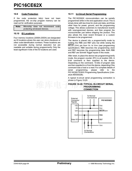
FIGURE 8-4:
COMPARATOR OUTPUT BLOCK DIAGRAM
Port Pins
MULTIPLEX
+
To RA3 or
RA4 Pin
Bus
Data
RD CMCON
Q
D
EN
-
Set
CMIF
Bit
Q
From
Other
Comparator
D
EN
CL
RD CMCON
NRESET
DS40182A-page 44
Preliminary
漏
1998 Microchip Technology Inc.


 1
1
 2
2
 3
3
 4
4
 5
5
 6
6
 7
7
 8
8
 9
9
 10
10
 11
11
 12
12
 13
13
 14
14
 15
15
 16
16
 17
17
 18
18
 19
19
 20
20
 21
21
 22
22
 23
23
 24
24
 25
25
 26
26
 27
27
 28
28
 29
29
 30
30
 31
31
 32
32
 33
33
 34
34
 35
35
 36
36
 37
37
 38
38
 39
39
 40
40
 41
41
 42
42
 43
43
 44
44
 45
45
 46
46
 47
47
 48
48
 49
49
 50
50
 51
51
 52
52
 53
53
 54
54
 55
55
 56
56
 57
57
 58
58
 59
59
 60
60
 61
61
 62
62
 63
63
 64
64
 65
65
 66
66
 67
67
 68
68
 69
69
 70
70
 71
71
 72
72
 73
73
 74
74
 75
75
 76
76
 77
77
 78
78
 79
79
 80
80
 81
81
 82
82
 83
83
 84
84
 85
85
 86
86
 87
87
 88
88
 89
89
 90
90
 91
91
 92
92
 93
93
 94
94
 95
95
 96
96
 97
97
 98
98
 99
99
 100
100
 101
101
 102
102
 103
103
 104
104
 105
105
 106
106
 107
107
 108
108
