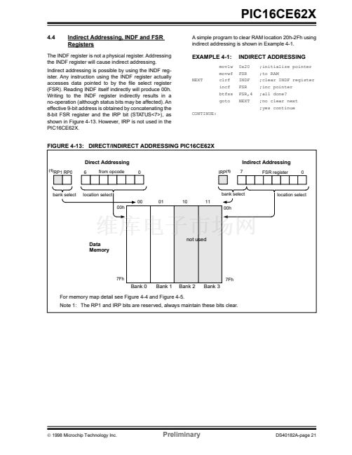
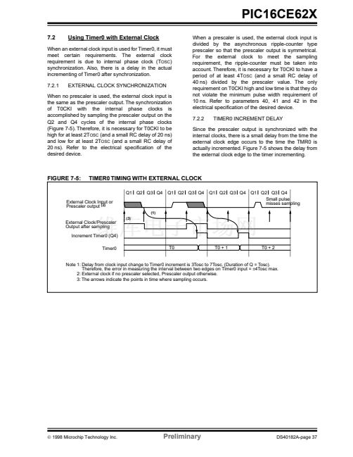
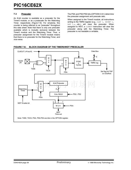
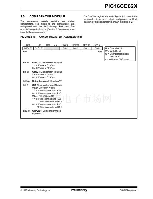
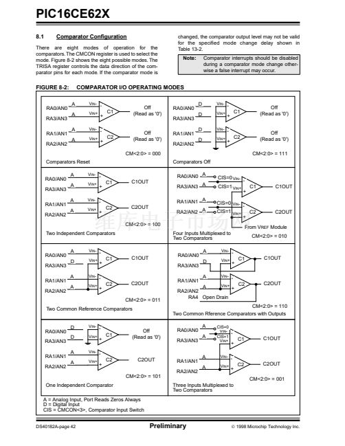
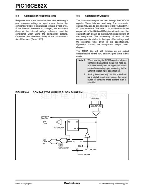
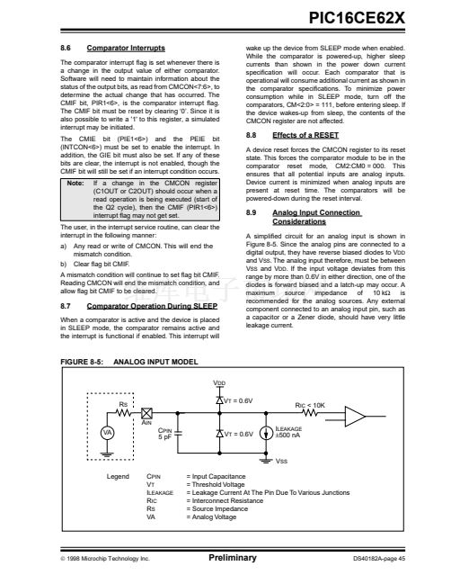
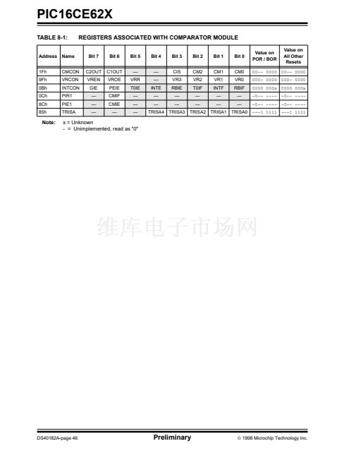
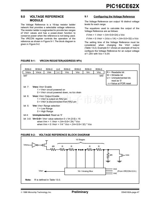
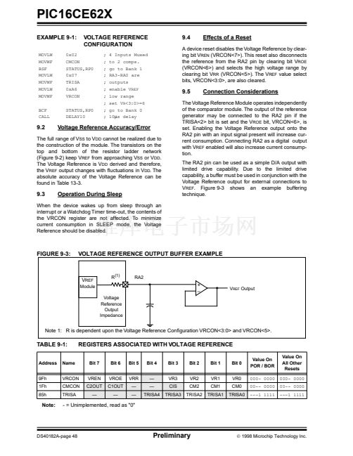
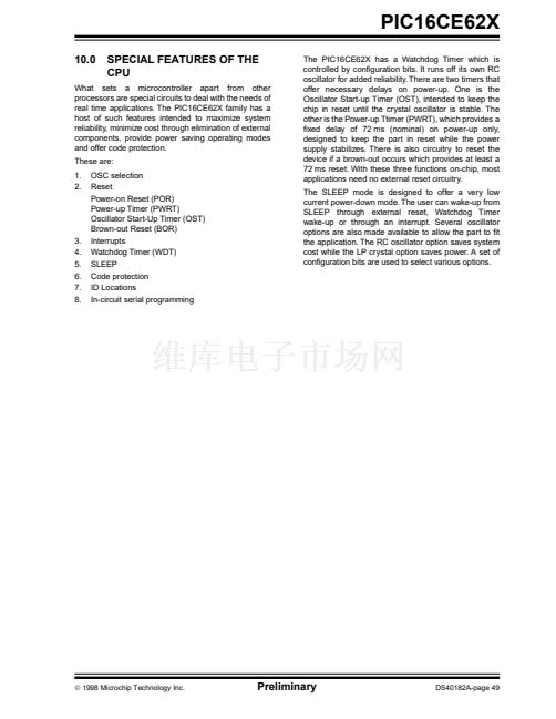
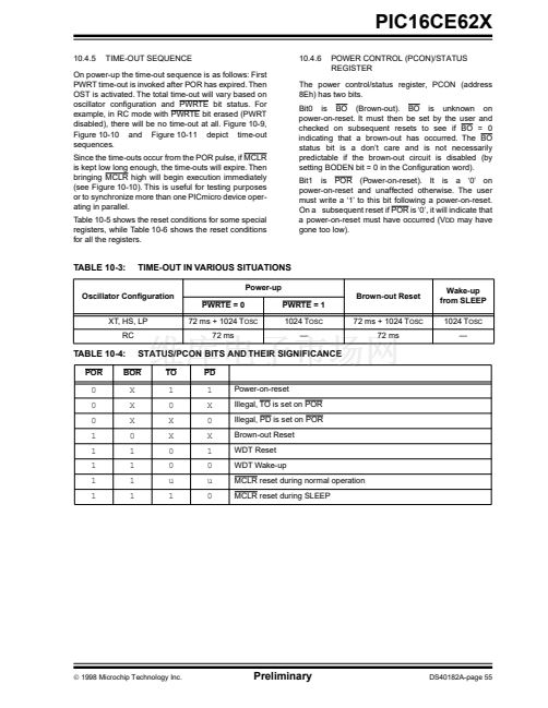
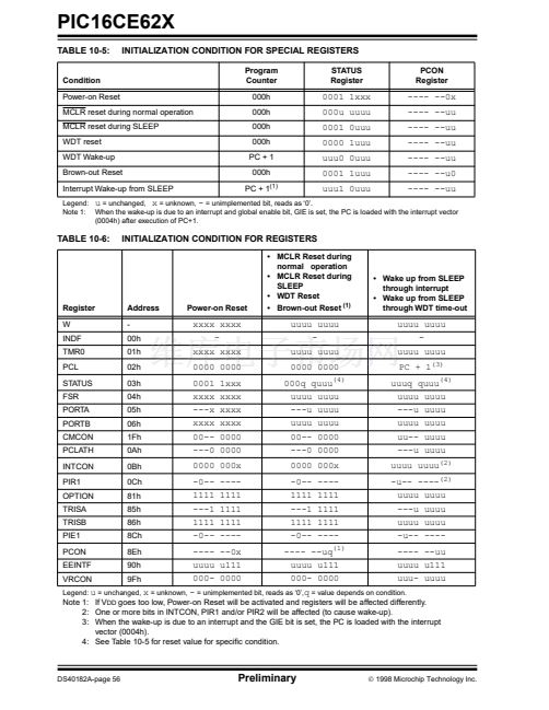
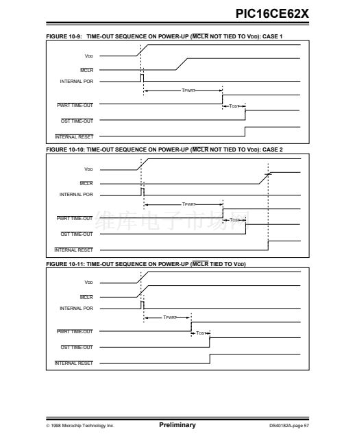
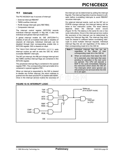
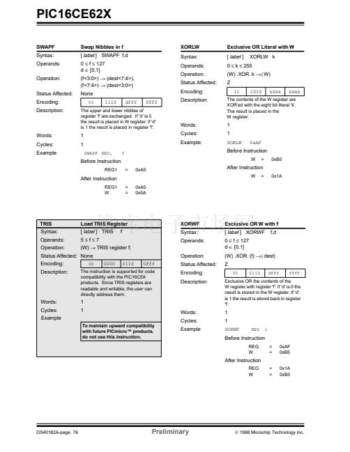
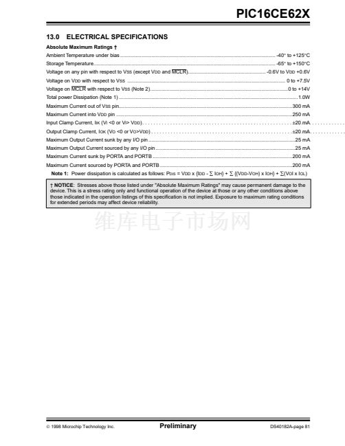
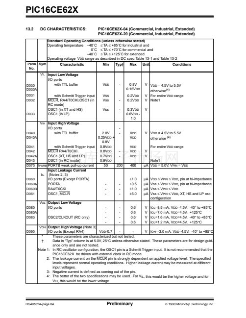
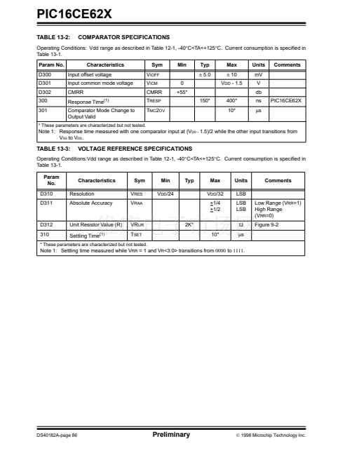
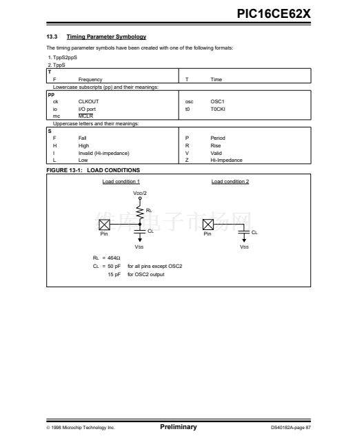
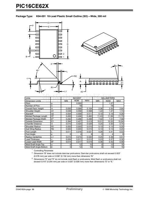
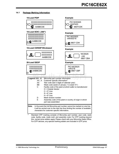
PIC16CE62X
3.0
ARCHITECTURAL OVERVIEW
The high performance of the PIC16CE62X family can
be attributed to a number of architectural features
commonly found in RISC microprocessors. To begin
with, the PIC16CE62X uses a Harvard architecture, in
which, program and data are accessed from separate
memories using separate busses. This improves
bandwidth over traditional von Neumann architecture
where program and data are fetched from the same
memory. Separating program and data memory further
allows instructions to be sized differently than 8-bit
wide data word. Instruction opcodes are 14-bits wide
making it possible to have all single word instructions.
A 14-bit wide program memory access bus fetches a
14-bit instruction in a single cycle. A two-stage pipeline
overlaps fetch and execution of instructions.
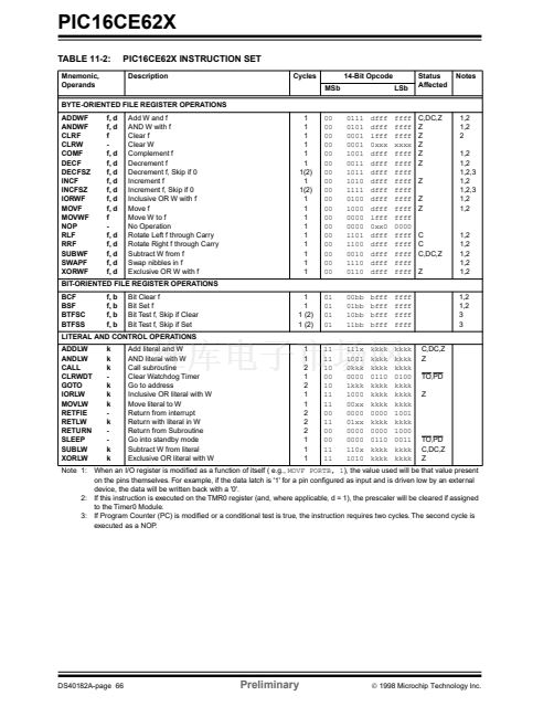
Consequently, all instructions (35) execute in a sin-
gle-cycle (200 ns @ 20 MHz) except for program
branches.
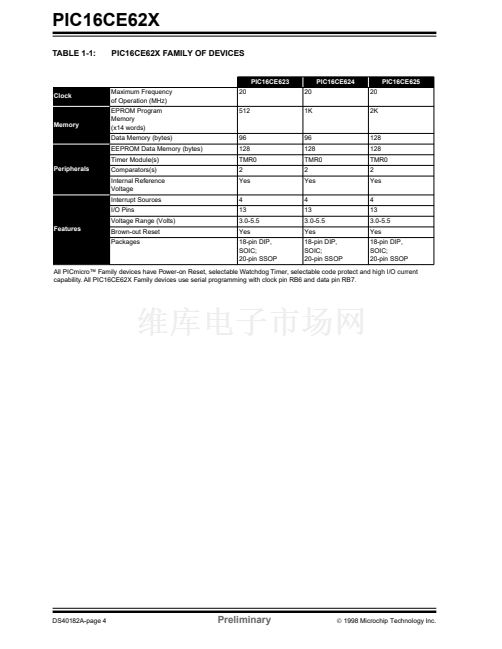
The PIC16CE623 addresses 512 x 14 on-chip program
memory. The PIC16CE624 addresses 1K x 14 program
memory. The PIC16CE625 addresses 2K x 14 program
memory. All program memory is internal.
The PIC16CE62X can directly or indirectly address its
register 铿乴es or data memory. All special function
registers including the program counter are mapped in
the data memory. The PIC16CE62X have an orthogo-
nal (symmetrical) instruction set that makes it possible
to carry out any operation on any register using any
addressing mode. This symmetrical nature and lack of
鈥榮pecial optimal situations鈥?make programming with the
PIC16CE62X simple yet ef铿乧ient. In addition, the
learning curve is reduced signi铿乧antly.
The PIC16CE62X devices contain an 8-bit ALU and
working register. The ALU is a general purpose
arithmetic unit. It performs arithmetic and Boolean
functions between data in the working register and any
register 铿乴e.
The ALU is 8-bit wide and capable of addition,
subtraction, shift and logical operations. Unless
otherwise mentioned, arithmetic operations are two's
complement in nature. In two-operand instructions,
typically one operand is the working register
(W register). The other operand is a 铿乴e register or an
immediate constant. In single operand instructions, the
operand is either the W register or a 铿乴e register.
The W register is an 8-bit working register used for ALU
operations. It is not an addressable register.
Depending on the instruction executed, the ALU may
affect the values of the Carry (C), Digit Carry (DC), and
Zero (Z) bits in the STATUS register. The C and DC bits
operate as a Borrow and Digit Borrow out bit,
respectively, bit in subtraction. See the
SUBLW
and
SUBWF
instructions for examples.
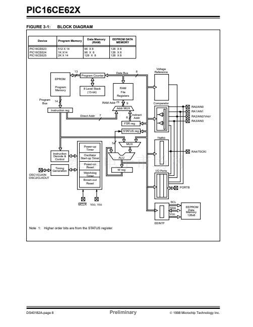
A simpli铿乪d block diagram is shown in Figure 3-1, with
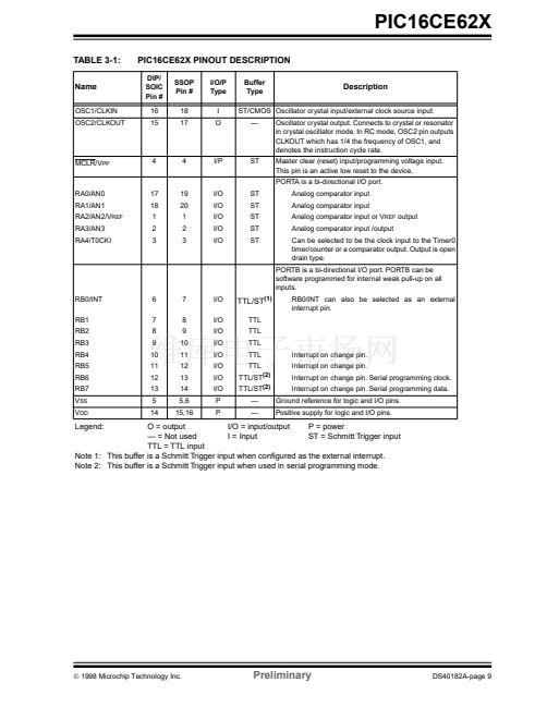
a description of the device pins in Table 3-1.
漏
1998 Microchip Technology Inc.
Preliminary
DS40182A-page 7


 1
1
 2
2
 3
3
 4
4
 5
5
 6
6
 7
7
 8
8
 9
9
 10
10
 11
11
 12
12
 13
13
 14
14
 15
15
 16
16
 17
17
 18
18
 19
19
 20
20
 21
21
 22
22
 23
23
 24
24
 25
25
 26
26
 27
27
 28
28
 29
29
 30
30
 31
31
 32
32
 33
33
 34
34
 35
35
 36
36
 37
37
 38
38
 39
39
 40
40
 41
41
 42
42
 43
43
 44
44
 45
45
 46
46
 47
47
 48
48
 49
49
 50
50
 51
51
 52
52
 53
53
 54
54
 55
55
 56
56
 57
57
 58
58
 59
59
 60
60
 61
61
 62
62
 63
63
 64
64
 65
65
 66
66
 67
67
 68
68
 69
69
 70
70
 71
71
 72
72
 73
73
 74
74
 75
75
 76
76
 77
77
 78
78
 79
79
 80
80
 81
81
 82
82
 83
83
 84
84
 85
85
 86
86
 87
87
 88
88
 89
89
 90
90
 91
91
 92
92
 93
93
 94
94
 95
95
 96
96
 97
97
 98
98
 99
99
 100
100
 101
101
 102
102
 103
103
 104
104
 105
105
 106
106
 107
107
 108
108
