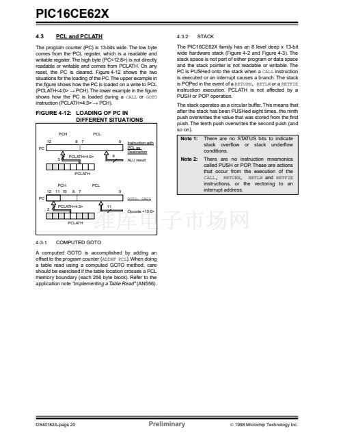
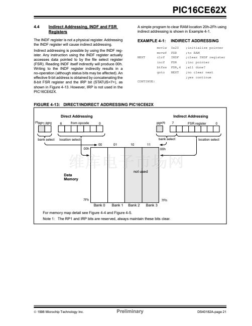
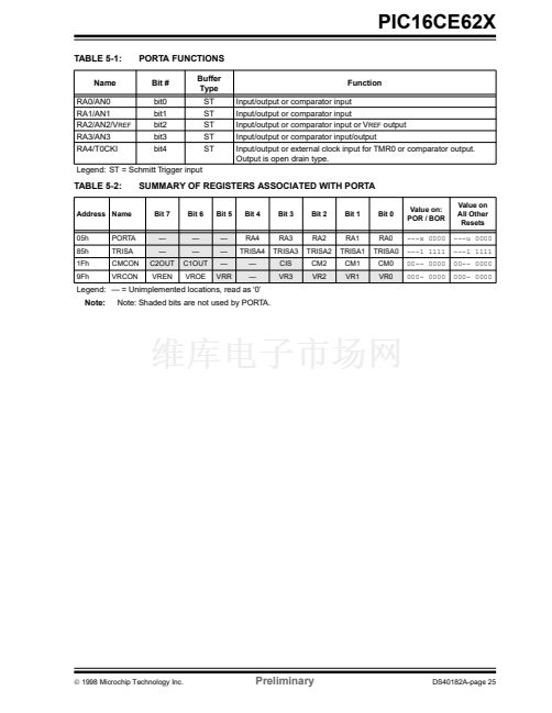
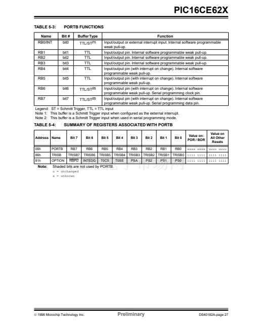
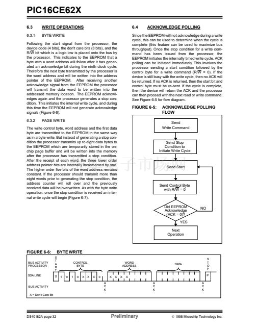
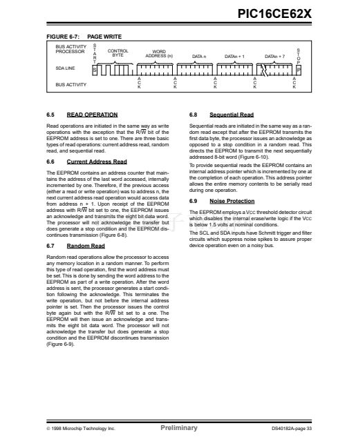
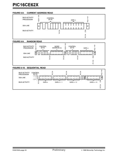
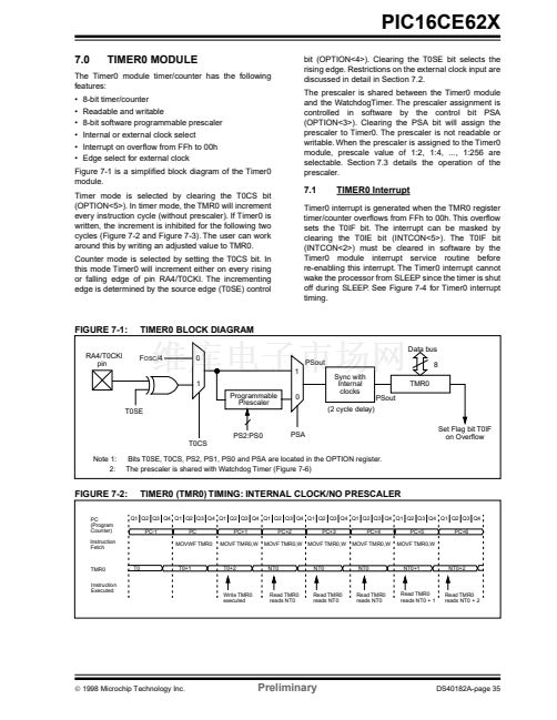
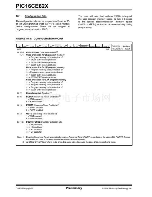
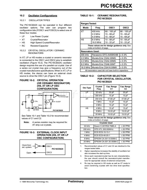
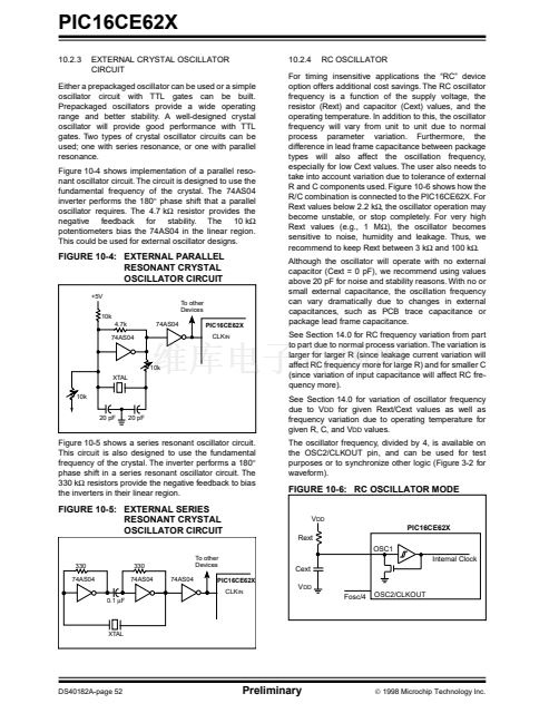
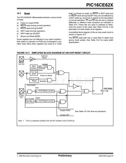
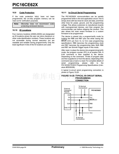
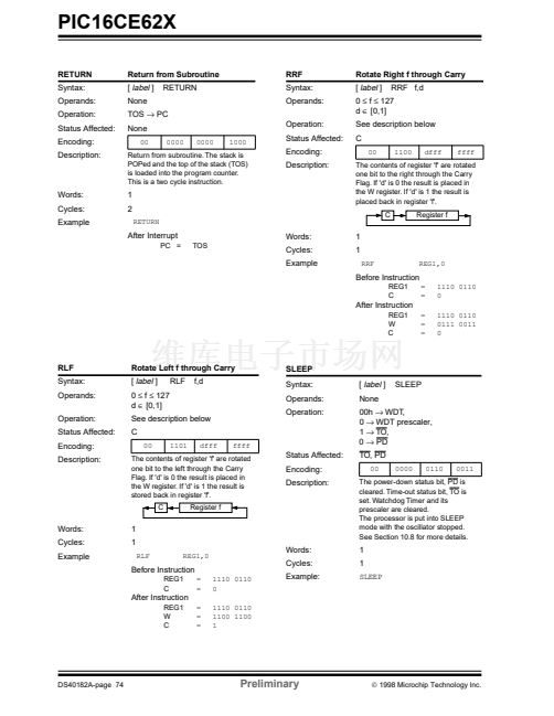
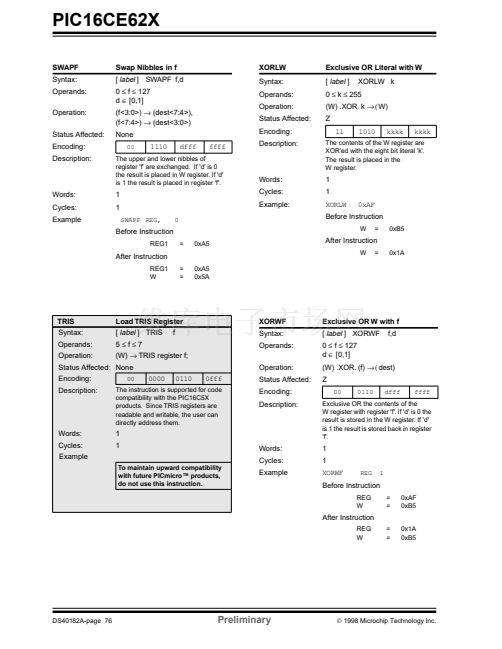
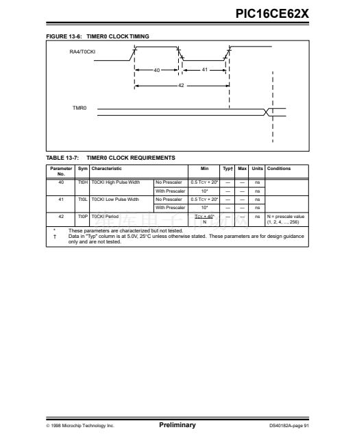
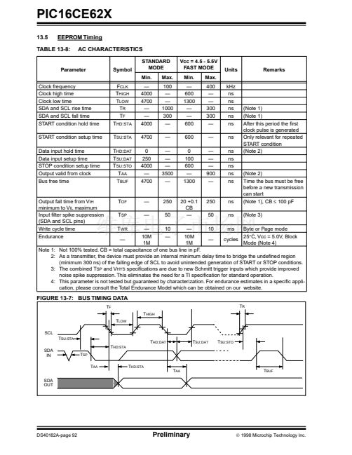
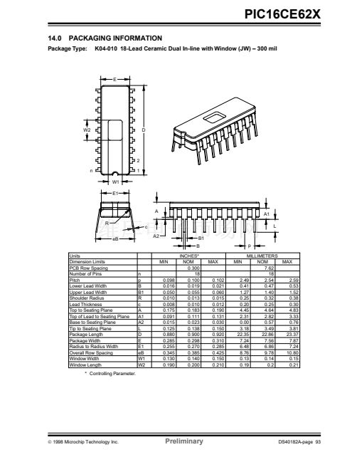
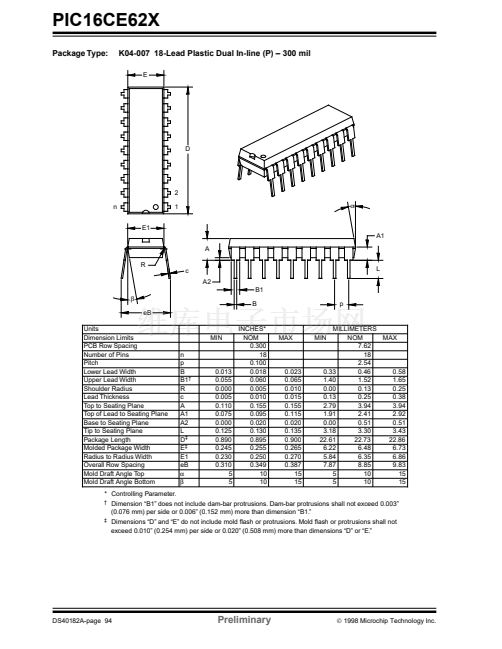
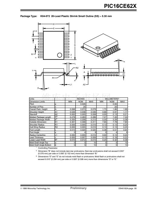
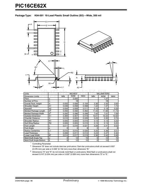
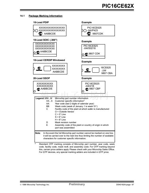
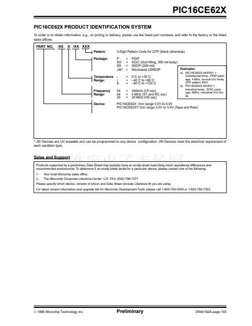
鈥?/div>
Units Conditions
MHz
MHz
kHz
MHz
MHz
MHz
kHz
ns
ns
碌s
ns
ns
ns
碌s
碌s
ns
碌s
ns
ns
ns
ns
XT and RC osc mode, V
DD
=5.0V
HS osc mode
LP osc mode
RC osc mode, V
DD
=5.0V
XT osc mode
HS osc mode
LP osc mode
XT and RC osc mode
HS osc mode
LP osc mode
RC osc mode
XT osc mode
HS osc mode
LP osc mode
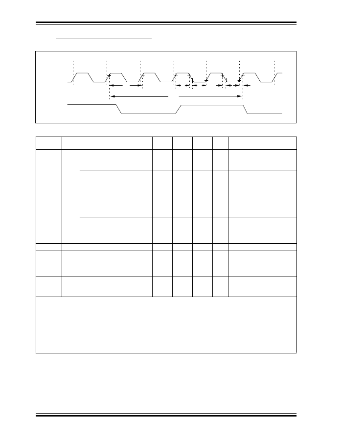
Sym
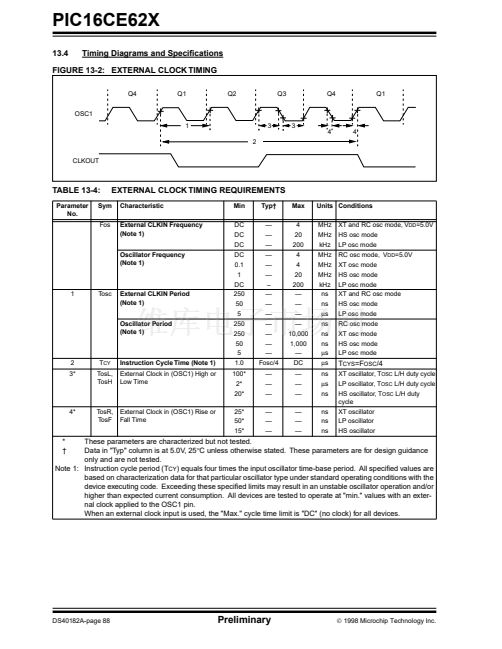
Fos
1
Tosc
External CLKIN Period
(Note 1)
Oscillator Period
(Note 1)
2
3*
T
CY
TosL,
TosH
Instruction Cycle Time (Note 1)
External Clock in (OSC1) High or
Low Time
T
CYS
=F
OSC
/4
XT oscillator, T
OSC
L/H duty cycle
LP oscillator, T
OSC
L/H duty cycle
HS oscillator, T
OSC
L/H duty
cycle
XT oscillator
LP oscillator
HS oscillator
4*
TosR,
TosF
External Clock in (OSC1) Rise or
Fall Time
25*
50*
15*
These parameters are characterized but not tested.
Data in "Typ" column is at 5.0V, 25掳C unless otherwise stated. These parameters are for design guidance
only and are not tested.
Note 1: Instruction cycle period (T
CY
) equals four times the input oscillator time-base period. All speci铿乪d values are
based on characterization data for that particular oscillator type under standard operating conditions with the
device executing code. Exceeding these speci铿乪d limits may result in an unstable oscillator operation and/or
higher than expected current consumption. All devices are tested to operate at "min." values with an exter-
nal clock applied to the OSC1 pin.
When an external clock input is used, the "Max." cycle time limit is "DC" (no clock) for all devices.
*
鈥?/div>
DS40182A-page 88
Preliminary
漏
1998 Microchip Technology Inc.


 1
1
 2
2
 3
3
 4
4
 5
5
 6
6
 7
7
 8
8
 9
9
 10
10
 11
11
 12
12
 13
13
 14
14
 15
15
 16
16
 17
17
 18
18
 19
19
 20
20
 21
21
 22
22
 23
23
 24
24
 25
25
 26
26
 27
27
 28
28
 29
29
 30
30
 31
31
 32
32
 33
33
 34
34
 35
35
 36
36
 37
37
 38
38
 39
39
 40
40
 41
41
 42
42
 43
43
 44
44
 45
45
 46
46
 47
47
 48
48
 49
49
 50
50
 51
51
 52
52
 53
53
 54
54
 55
55
 56
56
 57
57
 58
58
 59
59
 60
60
 61
61
 62
62
 63
63
 64
64
 65
65
 66
66
 67
67
 68
68
 69
69
 70
70
 71
71
 72
72
 73
73
 74
74
 75
75
 76
76
 77
77
 78
78
 79
79
 80
80
 81
81
 82
82
 83
83
 84
84
 85
85
 86
86
 87
87
 88
88
 89
89
 90
90
 91
91
 92
92
 93
93
 94
94
 95
95
 96
96
 97
97
 98
98
 99
99
 100
100
 101
101
 102
102
 103
103
 104
104
 105
105
 106
106
 107
107
 108
108
