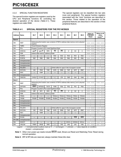
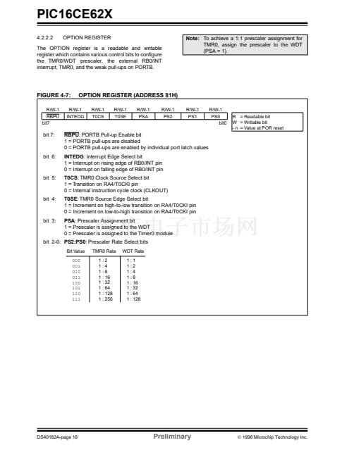
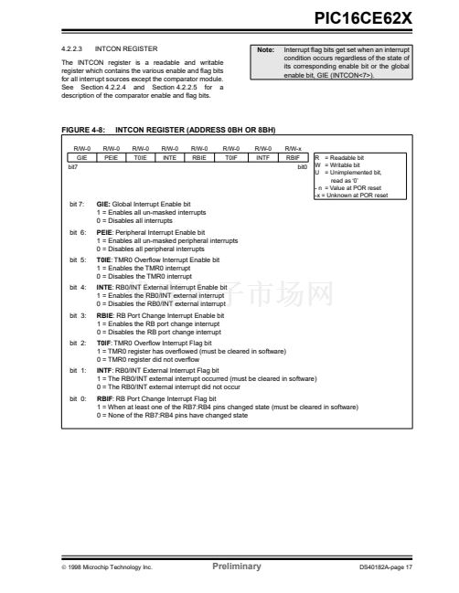
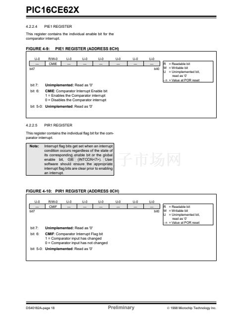
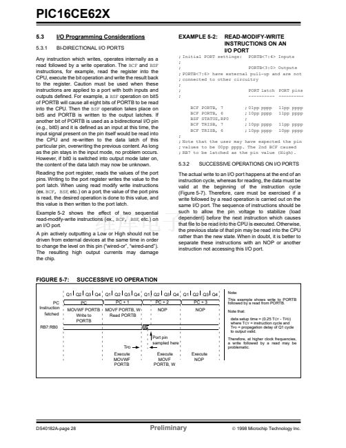
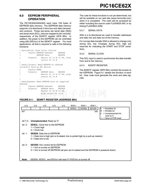
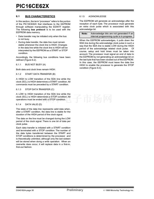
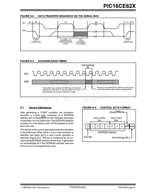
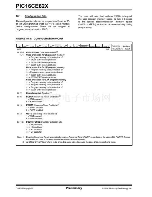
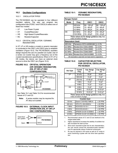
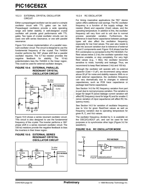
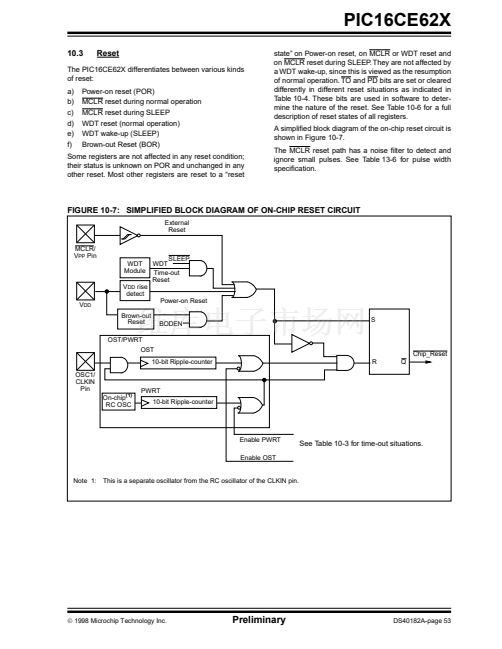
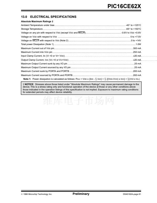
Absolute Maximum Ratings 鈥?/div>
Ambient Temperature under bias .............................................................................................................. -40掳 to +125掳C
Storage Temperature................................................................................................................................. -65掳 to +150掳C
Voltage on any pin with respect to V
SS
(except V
DD
and MCLR)....................................................... -0.6V to V
DD
+0.6V
Voltage on V
DD
with respect to V
SS
................................................................................................................ 0 to +7.5V
Voltage on MCLR with respect to V
SS
(Note 2)..................................................................................................0 to +14V
Total power Dissipation (Note 1) ...............................................................................................................................1.0W
Maximum Current out of V
SS
pin...........................................................................................................................300 mA
Maximum Current into V
DD
pin .............................................................................................................................250 mA
Input Clamp Current, I
IK
(V
I
<0 or V
I
> V
DD
)
......................................................................................................................卤20
mA
Output Clamp Current, I
OK
(V
O
<0 or V
O
>V
DD
)
...............................................................................................................卤20
mA
Maximum Output Current sunk by any I/O pin ........................................................................................................25 mA
Maximum Output Current sourced by any I/O pin ...................................................................................................25 mA
Maximum Current sunk by PORTA and PORTB ...................................................................................................200 mA
Maximum Current sourced by PORTA and PORTB ..............................................................................................200 mA
Note 1:
Power dissipation is calculated as follows: P
DIS
= V
DD
x {I
DD
-
鈭?/div>
I
OH
} +
鈭?/div>
{(V
DD
-V
OH
) x I
OH
} +
鈭?V
O
l x I
OL
)
鈥?/div>
NOTICE:
Stresses above those listed under "Absolute Maximum Ratings" may cause permanent damage to the
device. This is a stress rating only and functional operation of the device at those or any other conditions above
those indicated in the operation listings of this speci铿乧ation is not implied. Exposure to maximum rating conditions
for extended periods may affect device reliability.
漏
1998 Microchip Technology Inc.
Preliminary
DS40182A-page 81


 1
1
 2
2
 3
3
 4
4
 5
5
 6
6
 7
7
 8
8
 9
9
 10
10
 11
11
 12
12
 13
13
 14
14
 15
15
 16
16
 17
17
 18
18
 19
19
 20
20
 21
21
 22
22
 23
23
 24
24
 25
25
 26
26
 27
27
 28
28
 29
29
 30
30
 31
31
 32
32
 33
33
 34
34
 35
35
 36
36
 37
37
 38
38
 39
39
 40
40
 41
41
 42
42
 43
43
 44
44
 45
45
 46
46
 47
47
 48
48
 49
49
 50
50
 51
51
 52
52
 53
53
 54
54
 55
55
 56
56
 57
57
 58
58
 59
59
 60
60
 61
61
 62
62
 63
63
 64
64
 65
65
 66
66
 67
67
 68
68
 69
69
 70
70
 71
71
 72
72
 73
73
 74
74
 75
75
 76
76
 77
77
 78
78
 79
79
 80
80
 81
81
 82
82
 83
83
 84
84
 85
85
 86
86
 87
87
 88
88
 89
89
 90
90
 91
91
 92
92
 93
93
 94
94
 95
95
 96
96
 97
97
 98
98
 99
99
 100
100
 101
101
 102
102
 103
103
 104
104
 105
105
 106
106
 107
107
 108
108
