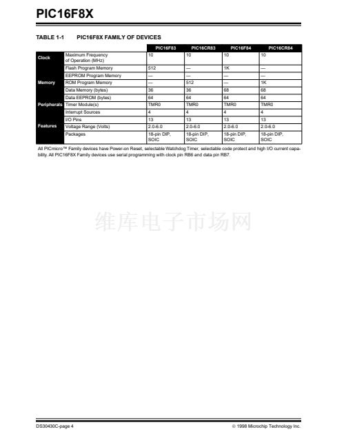
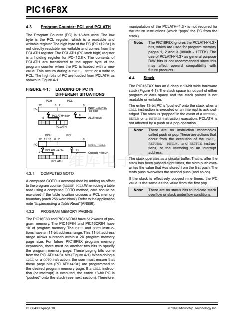
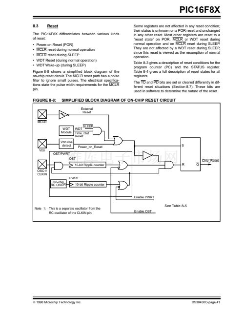
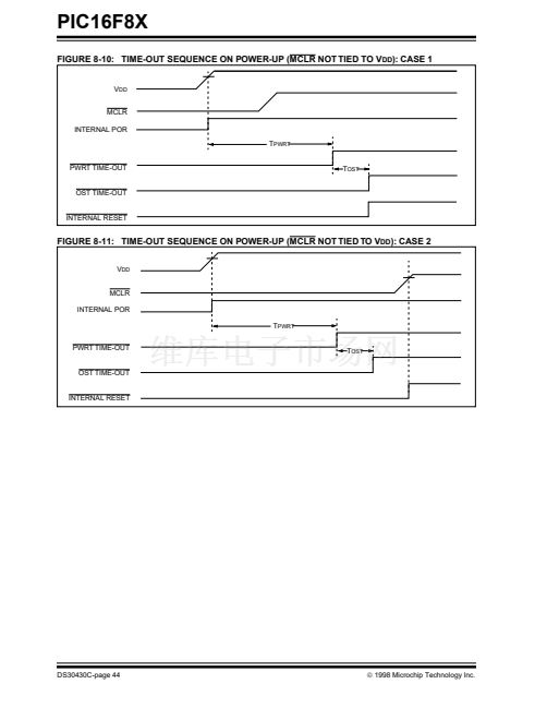
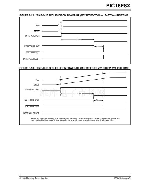
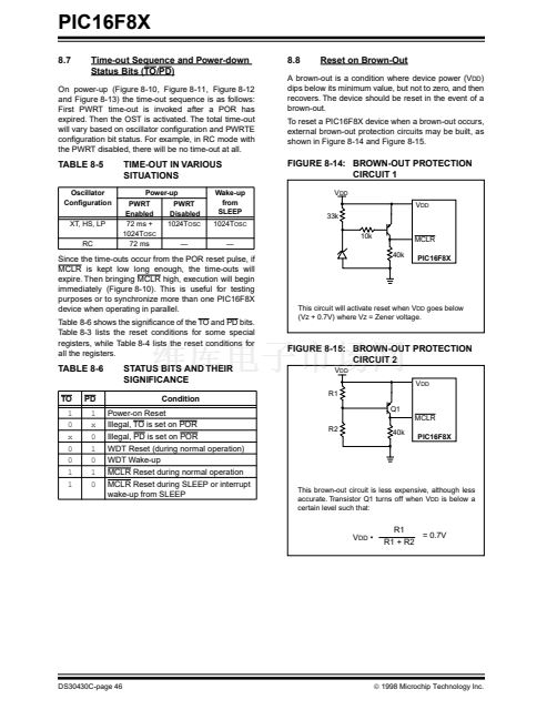
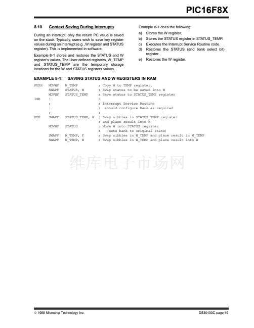
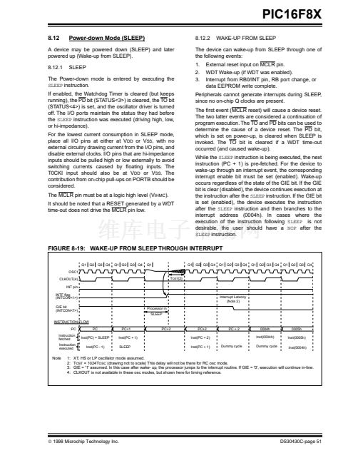
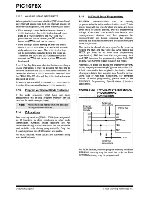
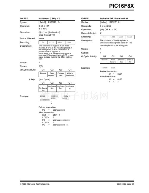
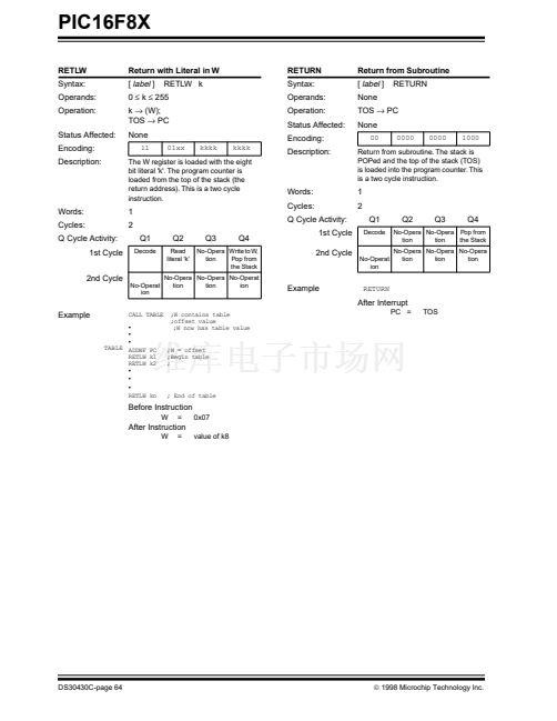
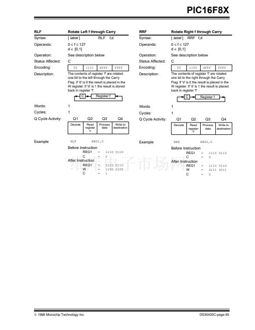
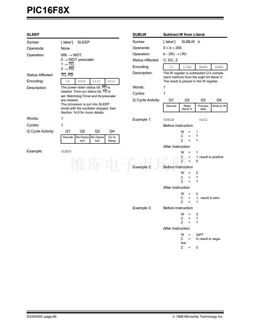
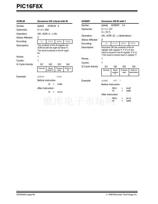
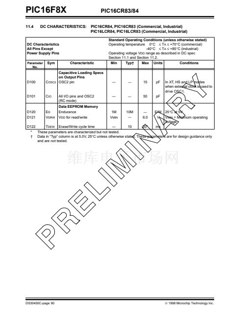
PIC16F8X
4.2.2.2
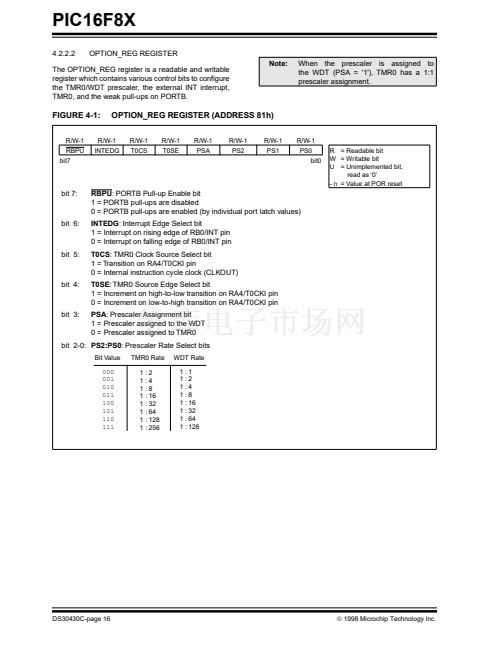
OPTION_REG REGISTER
Note:
When the prescaler is assigned to
the WDT (PSA = '1'), TMR0 has a 1:1
prescaler assignment.
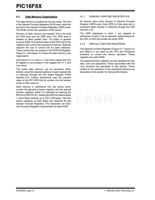
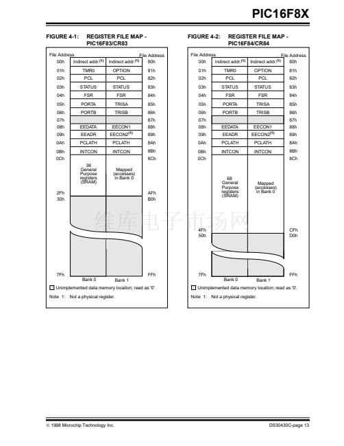
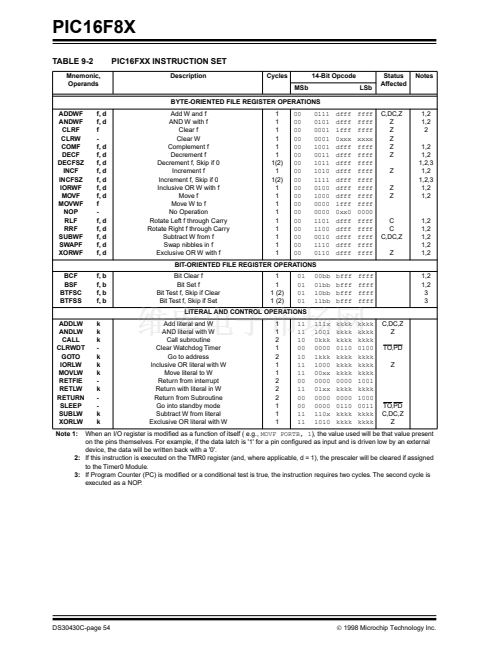
The OPTION_REG register is a readable and writable
register which contains various control bits to con铿乬ure
the TMR0/WDT prescaler, the external INT interrupt,
TMR0, and the weak pull-ups on PORTB.
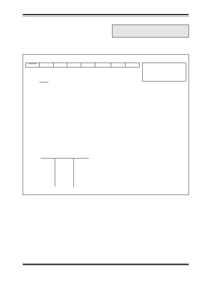
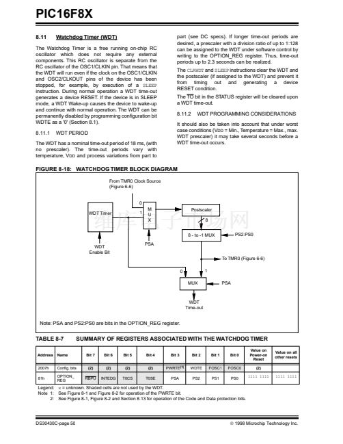
FIGURE 4-1:
R/W-1
RBPU
bit7
OPTION_REG REGISTER (ADDRESS 81h)
R/W-1
T0CS
R/W-1
T0SE
R/W-1
PSA
R/W-1
PS2
R/W-1
PS1
R/W-1
PS0
bit0
R/W-1
INTEDG
R = Readable bit
W = Writable bit
U = Unimplemented bit,
read as 鈥?鈥?/div>
- n = Value at POR reset
bit 7:
RBPU:
PORTB Pull-up Enable bit
1 = PORTB pull-ups are disabled
0 = PORTB pull-ups are enabled (by individual port latch values)
INTEDG:
Interrupt Edge Select bit
1 = Interrupt on rising edge of RB0/INT pin
0 = Interrupt on falling edge of RB0/INT pin
T0CS:
TMR0 Clock Source Select bit
1 = Transition on RA4/T0CKI pin
0 = Internal instruction cycle clock (CLKOUT)
T0SE:
TMR0 Source Edge Select bit
1 = Increment on high-to-low transition on RA4/T0CKI pin
0 = Increment on low-to-high transition on RA4/T0CKI pin
PSA:
Prescaler Assignment bit
1 = Prescaler assigned to the WDT
0 = Prescaler assigned to TMR0
bit 6:
bit 5:
bit 4:
bit 3:
bit 2-0:
PS2:PS0:
Prescaler Rate Select bits
Bit Value
000
001
010
011
100
101
110
111
TMR0 Rate
1:2
1:4
1:8
1 : 16
1 : 32
1 : 64
1 : 128
1 : 256
WDT Rate
1:1
1:2
1:4
1:8
1 : 16
1 : 32
1 : 64
1 : 128
DS30430C-page 16
漏
1998 Microchip Technology Inc.


 1
1
 2
2
 3
3
 4
4
 5
5
 6
6
 7
7
 8
8
 9
9
 10
10
 11
11
 12
12
 13
13
 14
14
 15
15
 16
16
 17
17
 18
18
 19
19
 20
20
 21
21
 22
22
 23
23
 24
24
 25
25
 26
26
 27
27
 28
28
 29
29
 30
30
 31
31
 32
32
 33
33
 34
34
 35
35
 36
36
 37
37
 38
38
 39
39
 40
40
 41
41
 42
42
 43
43
 44
44
 45
45
 46
46
 47
47
 48
48
 49
49
 50
50
 51
51
 52
52
 53
53
 54
54
 55
55
 56
56
 57
57
 58
58
 59
59
 60
60
 61
61
 62
62
 63
63
 64
64
 65
65
 66
66
 67
67
 68
68
 69
69
 70
70
 71
71
 72
72
 73
73
 74
74
 75
75
 76
76
 77
77
 78
78
 79
79
 80
80
 81
81
 82
82
 83
83
 84
84
 85
85
 86
86
 87
87
 88
88
 89
89
 90
90
 91
91
 92
92
 93
93
 94
94
 95
95
 96
96
 97
97
 98
98
 99
99
 100
100
 101
101
 102
102
 103
103
 104
104
 105
105
 106
106
 107
107
 108
108
 109
109
 110
110
 111
111
 112
112
 113
113
 114
114
 115
115
 116
116
 117
117
 118
118
 119
119
 120
120
 121
121
 122
122
 123
123
 124
124
