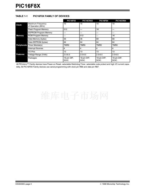
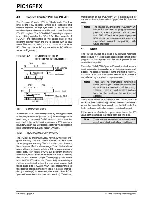
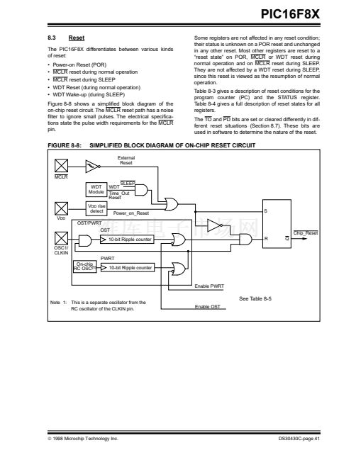
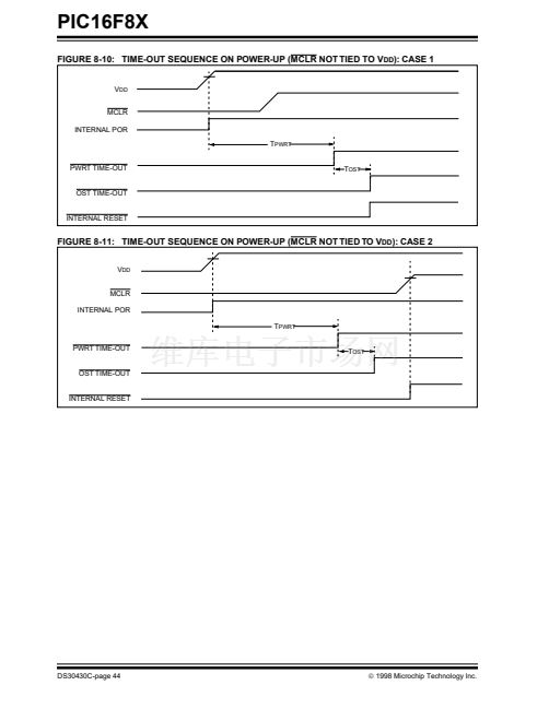
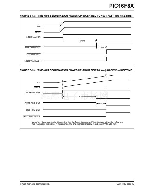
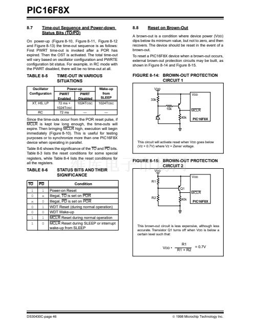
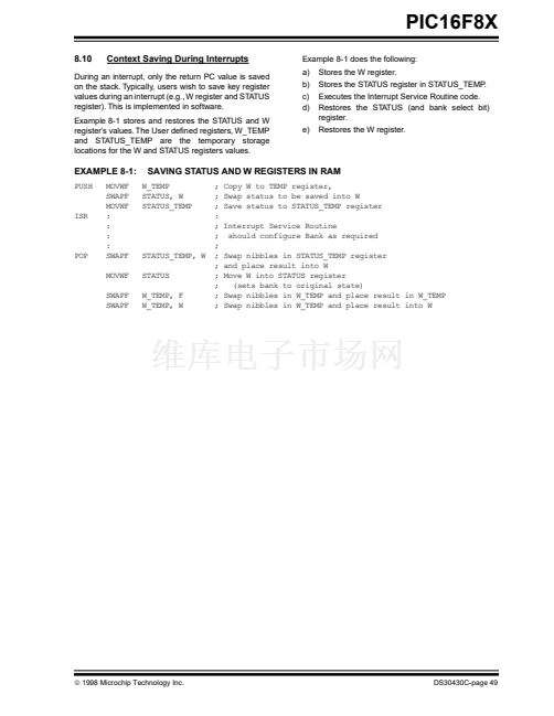
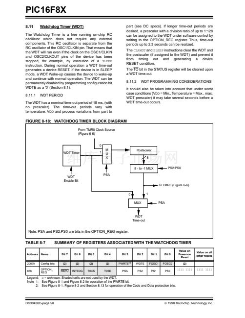
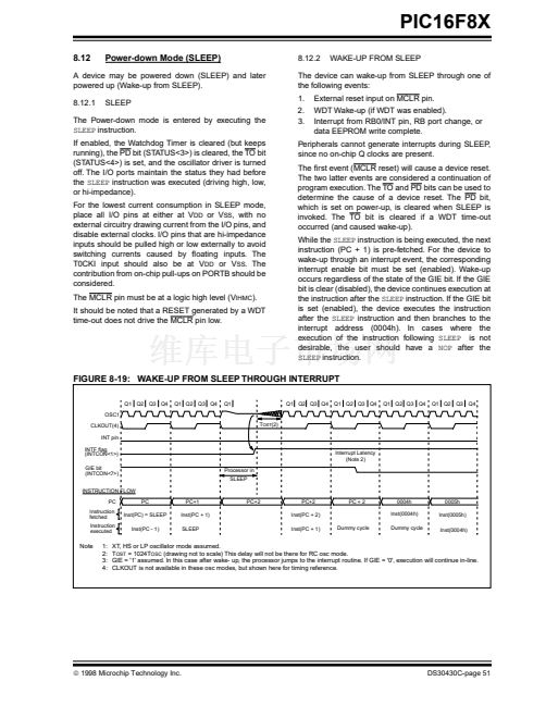
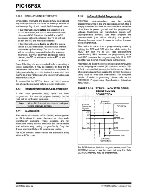
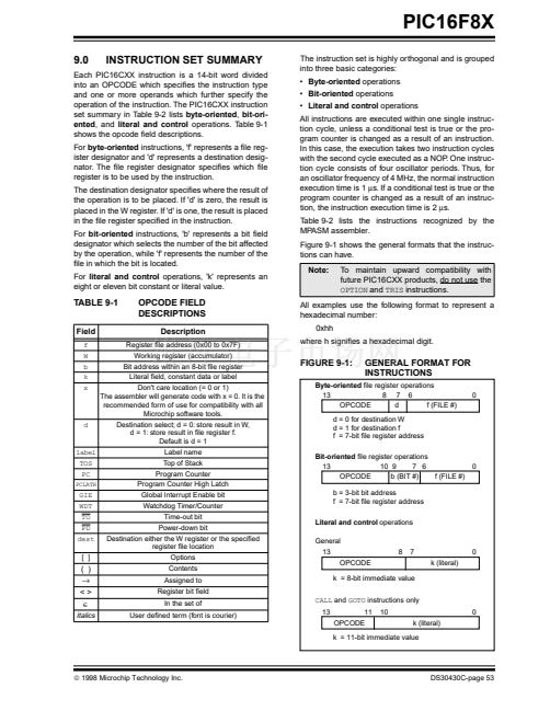
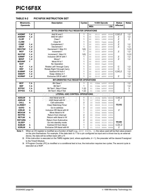
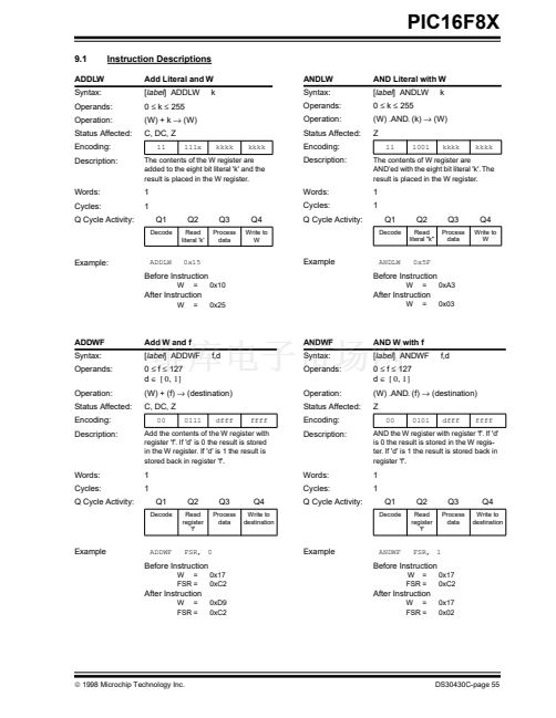
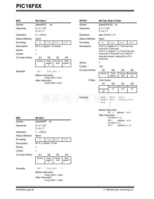
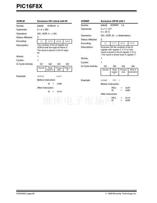
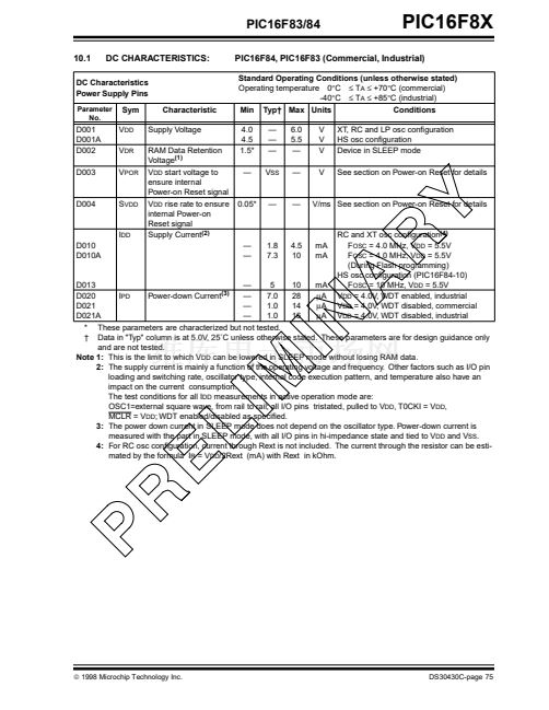
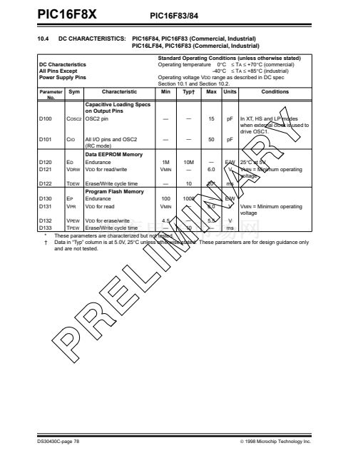
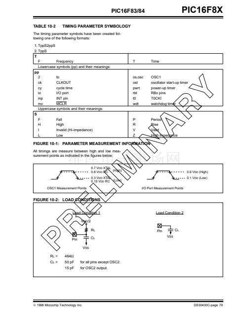
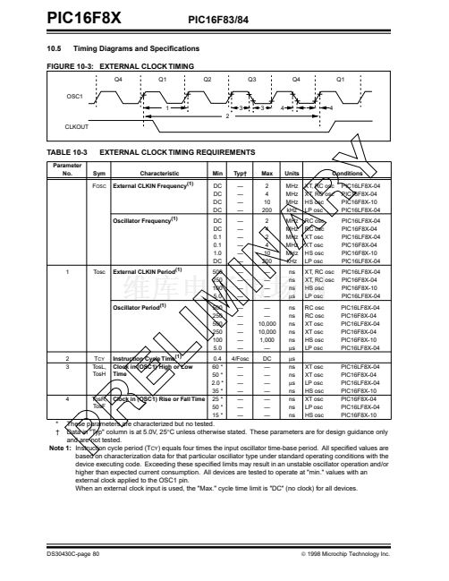
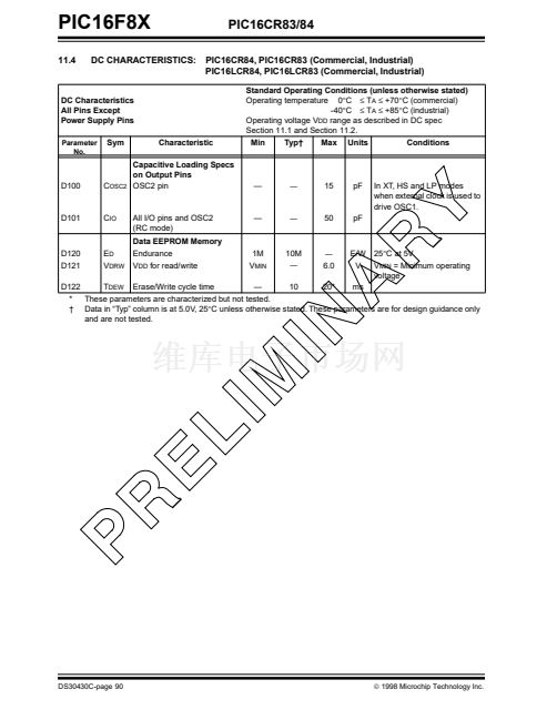
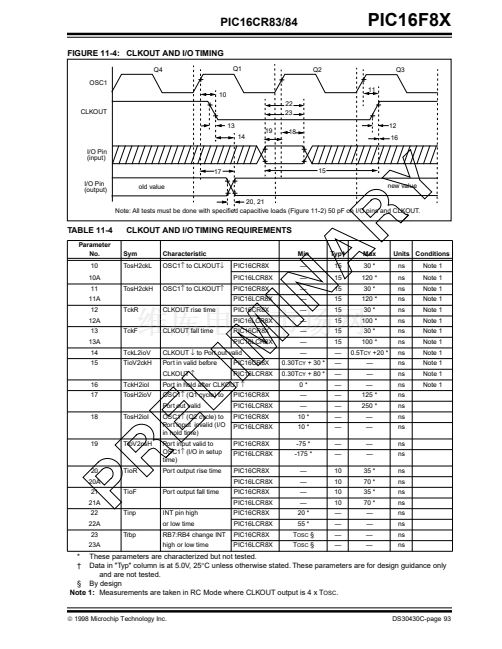
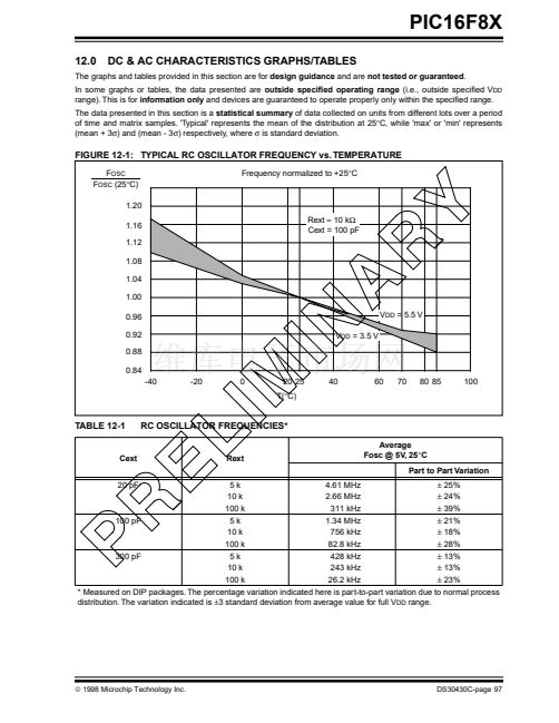
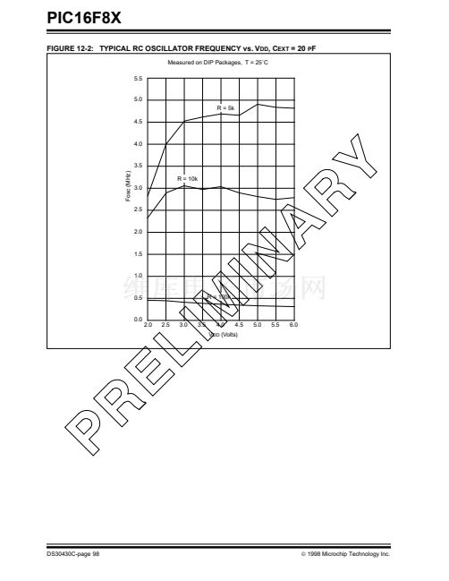
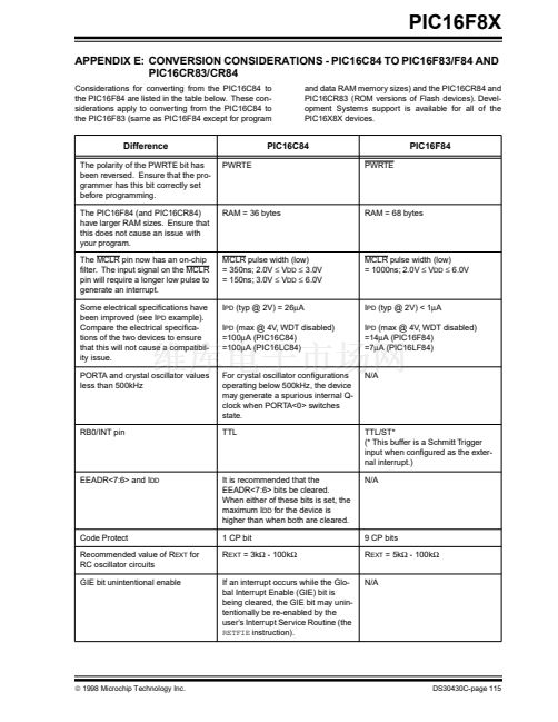
PIC16F8X
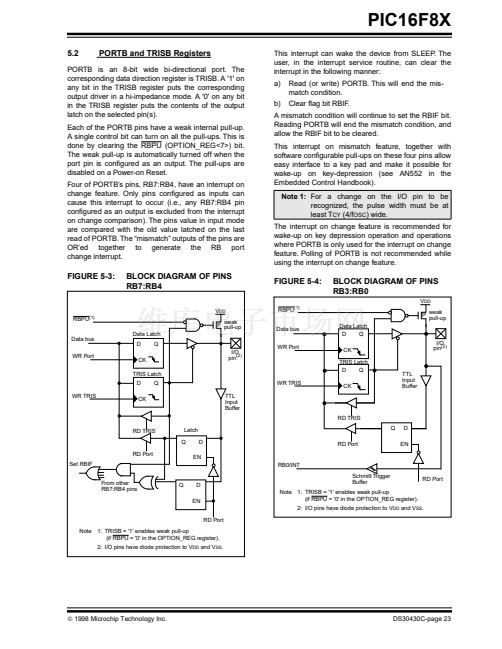
5.2
PORTB and TRISB Registers
PORTB is an 8-bit wide bi-directional port. The
corresponding data direction register is TRISB. A '1' on
any bit in the TRISB register puts the corresponding
output driver in a hi-impedance mode. A '0' on any bit
in the TRISB register puts the contents of the output
latch on the selected pin(s).
Each of the PORTB pins have a weak internal pull-up.
A single control bit can turn on all the pull-ups. This is
done by clearing the RBPU (OPTION_REG<7>) bit.
The weak pull-up is automatically turned off when the
port pin is con铿乬ured as an output. The pull-ups are
disabled on a Power-on Reset.
Four of PORTB鈥檚 pins, RB7:RB4, have an interrupt on
change feature. Only pins con铿乬ured as inputs can
cause this interrupt to occur (i.e., any RB7:RB4 pin
con铿乬ured as an output is excluded from the interrupt
on change comparison). The pins value in input mode
are compared with the old value latched on the last
read of PORTB. The 鈥渕ismatch鈥?outputs of the pins are
OR鈥檈d together to generate the RB port
change interrupt.
This interrupt can wake the device from SLEEP. The
user, in the interrupt service routine, can clear the
interrupt in the following manner:
a)
b)
Read (or write) PORTB. This will end the mis-
match condition.
Clear 铿俛g bit RBIF.
A mismatch condition will continue to set the RBIF bit.
Reading PORTB will end the mismatch condition, and
allow the RBIF bit to be cleared.
This interrupt on mismatch feature, together with
software con铿乬urable pull-ups on these four pins allow
easy interface to a key pad and make it possible for
wake-up on key-depression (see AN552 in the
Embedded Control Handbook).
Note 1:
For a change on the I/O pin to be
recognized, the pulse width must be at
least T
CY
(4/f
OSC
) wide.
The interrupt on change feature is recommended for
wake-up on key depression operation and operations
where PORTB is only used for the interrupt on change
feature. Polling of PORTB is not recommended while
using the interrupt on change feature.
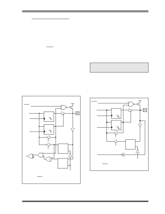
FIGURE 5-3:
BLOCK DIAGRAM OF PINS
RB7:RB4
V
DD
FIGURE 5-4:
RBPU
(1)
BLOCK DIAGRAM OF PINS
RB3:RB0
V
DD
weak
P pull-up
Data Latch
D
Q
CK
TRIS Latch
D
Q
I/O
pin
(2)
RBPU
(1)
Data Latch
D
CK
TRIS Latch
D
WR TRIS
CK
Q
Q
weak
P pull-up
Data bus
WR Port
Data bus
WR Port
I/O
pin
(2)
WR TRIS
TTL
Input
Buffer
CK
TTL
Input
Buffer
RD TRIS
RD TRIS
Latch
Q
RD Port
Set RBIF
From other
RB7:RB4 pins
D
EN
RB0/INT
Schmitt Trigger
Buffer
Note 1: TRISB = '1' enables weak pull-up
(if RBPU = '0' in the OPTION_REG register).
2: I/O pins have diode protection to V
DD
and V
SS
.
RD Port
Note 1: TRISB = '1' enables weak pull-up
(if RBPU = '0' in the OPTION_REG register).
2: I/O pins have diode protection to V
DD
and V
SS
.
RD Port
RD Port
Q
D
EN
Q
D
EN
漏
1998 Microchip Technology Inc.
DS30430C-page 23


 1
1
 2
2
 3
3
 4
4
 5
5
 6
6
 7
7
 8
8
 9
9
 10
10
 11
11
 12
12
 13
13
 14
14
 15
15
 16
16
 17
17
 18
18
 19
19
 20
20
 21
21
 22
22
 23
23
 24
24
 25
25
 26
26
 27
27
 28
28
 29
29
 30
30
 31
31
 32
32
 33
33
 34
34
 35
35
 36
36
 37
37
 38
38
 39
39
 40
40
 41
41
 42
42
 43
43
 44
44
 45
45
 46
46
 47
47
 48
48
 49
49
 50
50
 51
51
 52
52
 53
53
 54
54
 55
55
 56
56
 57
57
 58
58
 59
59
 60
60
 61
61
 62
62
 63
63
 64
64
 65
65
 66
66
 67
67
 68
68
 69
69
 70
70
 71
71
 72
72
 73
73
 74
74
 75
75
 76
76
 77
77
 78
78
 79
79
 80
80
 81
81
 82
82
 83
83
 84
84
 85
85
 86
86
 87
87
 88
88
 89
89
 90
90
 91
91
 92
92
 93
93
 94
94
 95
95
 96
96
 97
97
 98
98
 99
99
 100
100
 101
101
 102
102
 103
103
 104
104
 105
105
 106
106
 107
107
 108
108
 109
109
 110
110
 111
111
 112
112
 113
113
 114
114
 115
115
 116
116
 117
117
 118
118
 119
119
 120
120
 121
121
 122
122
 123
123
 124
124
