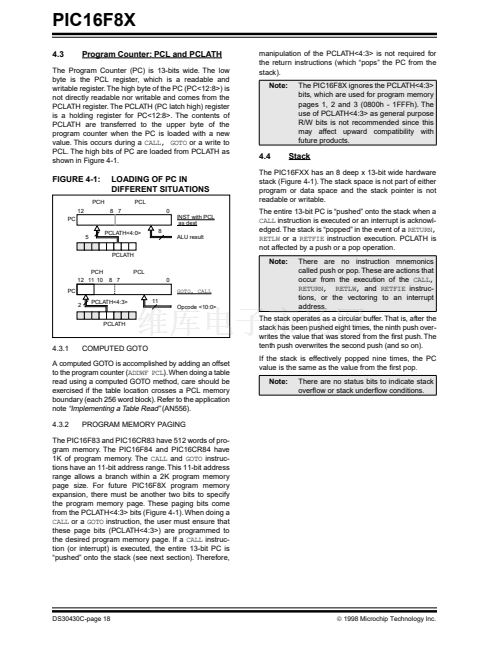
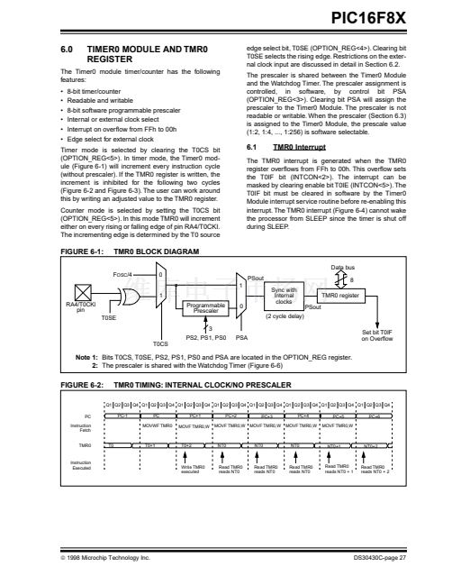
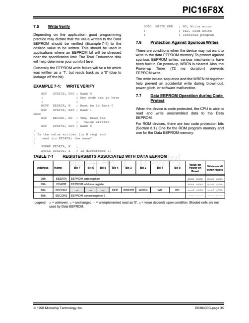
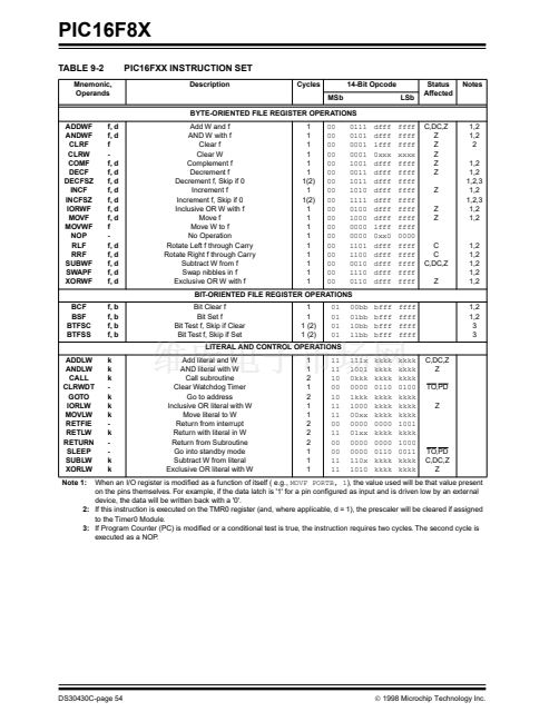
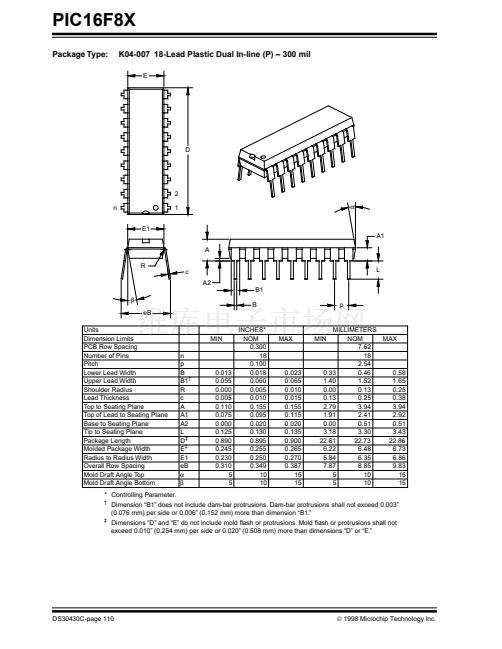
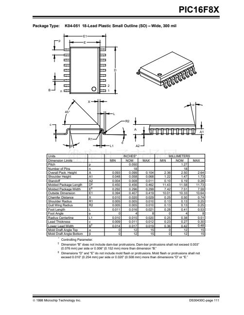
鈥?/div>
Dummy Cycle
0004h
Inst (0004h)
Dummy Cycle
0005h
Inst (0005h)
Inst (0004h)
1
5
Q2
Q3
Q4
Q1
Q2
Q3
Q4
Q1
Q2
Q3
Q4
Q1
Q2
Q3
Q4
Q1
Q2
Q3
Q4
4
1
Interrupt Latency 2
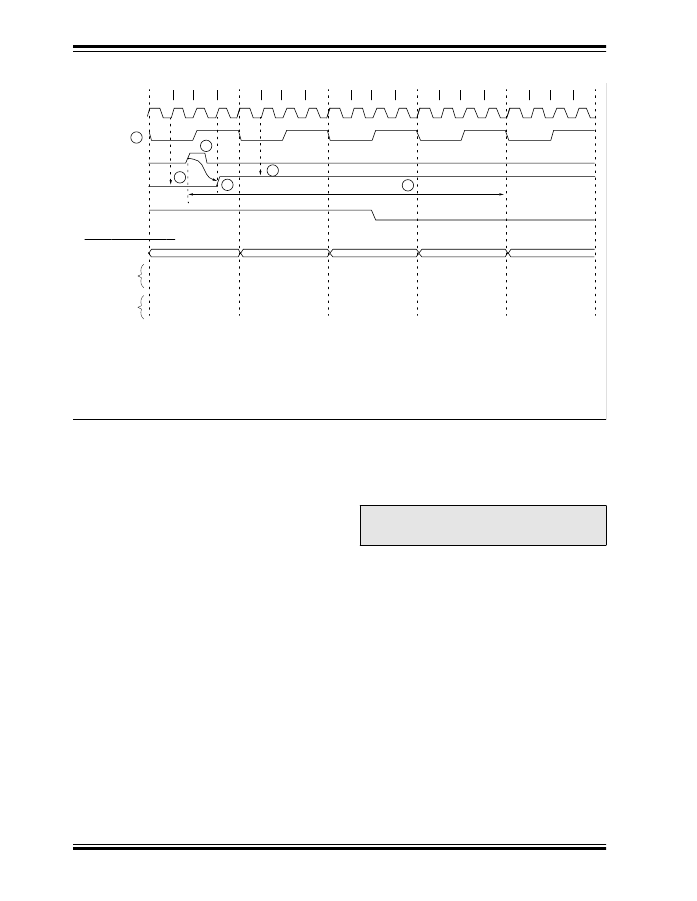
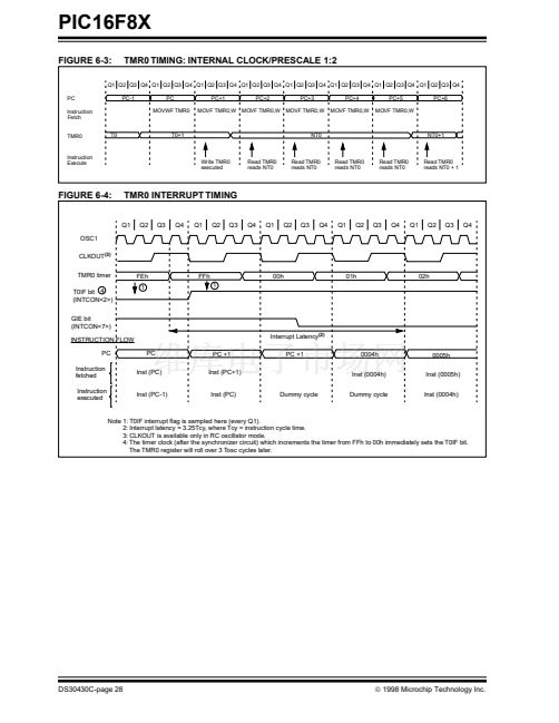
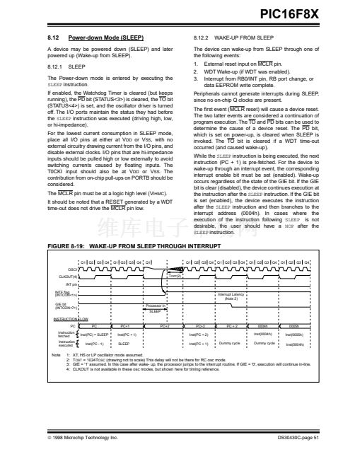
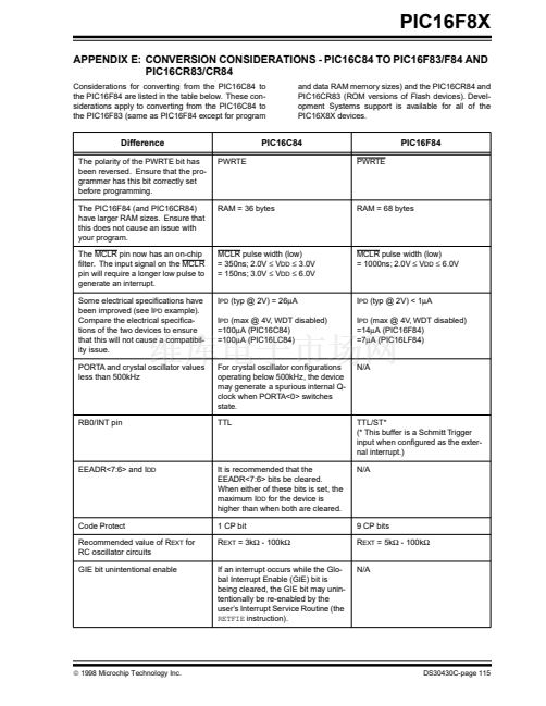
Note 1: INTF 铿俛g is sampled here (every Q1).
2: Interrupt latency = 3-4Tcy where Tcy = instruction cycle time.
Latency is the same whether Inst (PC) is a single cycle or a 2-cycle instruction.
3: CLKOUT is available only in RC oscillator mode.
4: For minimum width of INT pulse, refer to AC specs.
5: INTF is enabled to be set anytime during the Q4-Q1 cycles.
8.9.1
INT INTERRUPT
8.9.3
PORT RB INTERRUPT
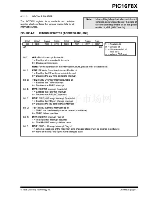
External interrupt on RB0/INT pin is edge triggered:
either rising if INTEDG bit (OPTION_REG<6>) is set,
or falling, if INTEDG bit is clear. When a valid edge
appears on the RB0/INT pin, the INTF bit
(INTCON<1>) is set. This interrupt can be disabled by
clearing control bit INTE (INTCON<4>). Flag bit INTF
must be cleared in software via the interrupt service
routine before re-enabling this interrupt. The INT
interrupt can wake the processor from SLEEP
(Section 8.12) only if the INTE bit was set prior to going
into SLEEP. The status of the GIE bit decides whether
the processor branches to the interrupt vector
following wake-up.
8.9.2
TMR0 INTERRUPT
An input change on PORTB<7:4> sets 铿俛g bit RBIF
(INTCON<0>). The interrupt can be enabled/disabled
by setting/clearing enable bit RBIE (INTCON<3>)
(Section 5.2).
Note 1:
For a change on the I/O pin to be
recognized, the pulse width must be at
least T
CY
wide.
An over铿俹w (FFh
鈫?/div>
00h) in TMR0 will set 铿俛g bit T0IF
(INTCON<2>). The interrupt can be enabled/disabled
by setting/clearing enable bit T0IE (INTCON<5>)
(Section 6.0).
DS30430C-page 48
漏
1998 Microchip Technology Inc.


 1
1
 2
2
 3
3
 4
4
 5
5
 6
6
 7
7
 8
8
 9
9
 10
10
 11
11
 12
12
 13
13
 14
14
 15
15
 16
16
 17
17
 18
18
 19
19
 20
20
 21
21
 22
22
 23
23
 24
24
 25
25
 26
26
 27
27
 28
28
 29
29
 30
30
 31
31
 32
32
 33
33
 34
34
 35
35
 36
36
 37
37
 38
38
 39
39
 40
40
 41
41
 42
42
 43
43
 44
44
 45
45
 46
46
 47
47
 48
48
 49
49
 50
50
 51
51
 52
52
 53
53
 54
54
 55
55
 56
56
 57
57
 58
58
 59
59
 60
60
 61
61
 62
62
 63
63
 64
64
 65
65
 66
66
 67
67
 68
68
 69
69
 70
70
 71
71
 72
72
 73
73
 74
74
 75
75
 76
76
 77
77
 78
78
 79
79
 80
80
 81
81
 82
82
 83
83
 84
84
 85
85
 86
86
 87
87
 88
88
 89
89
 90
90
 91
91
 92
92
 93
93
 94
94
 95
95
 96
96
 97
97
 98
98
 99
99
 100
100
 101
101
 102
102
 103
103
 104
104
 105
105
 106
106
 107
107
 108
108
 109
109
 110
110
 111
111
 112
112
 113
113
 114
114
 115
115
 116
116
 117
117
 118
118
 119
119
 120
120
 121
121
 122
122
 123
123
 124
124
