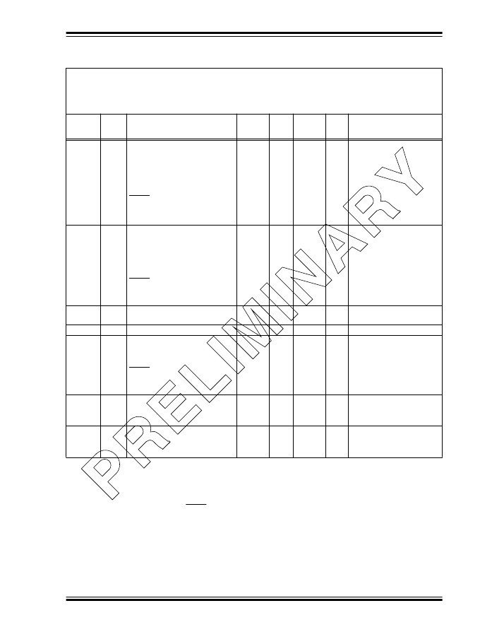
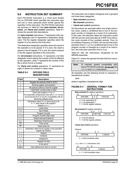
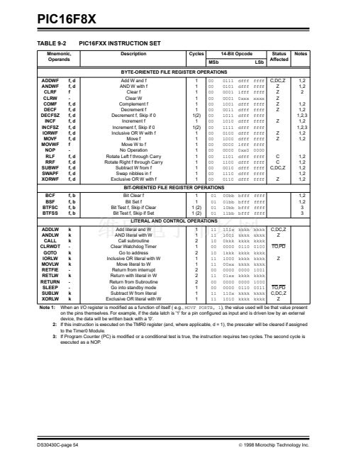
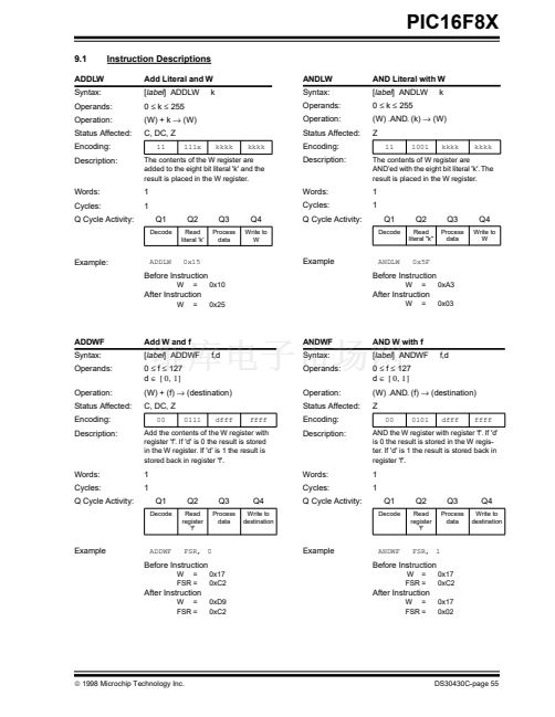
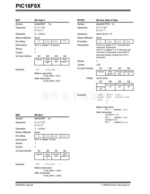
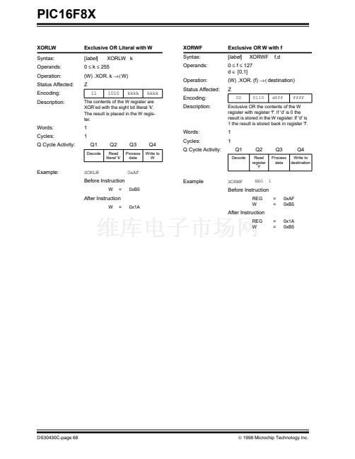
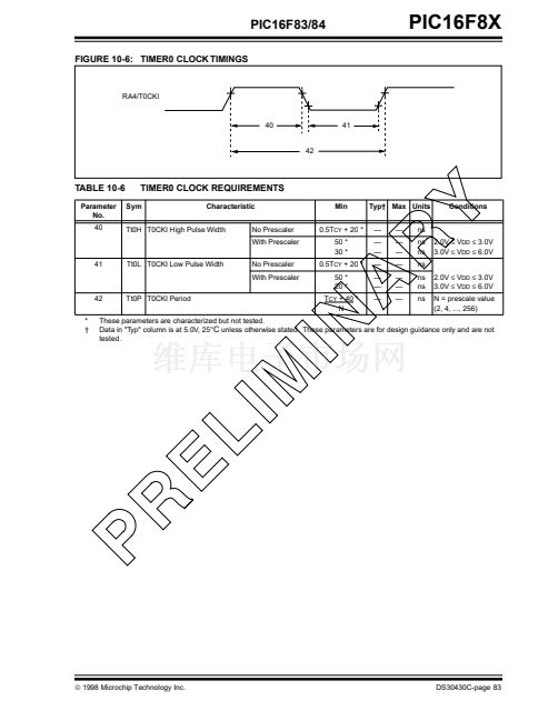
鈥?/div>
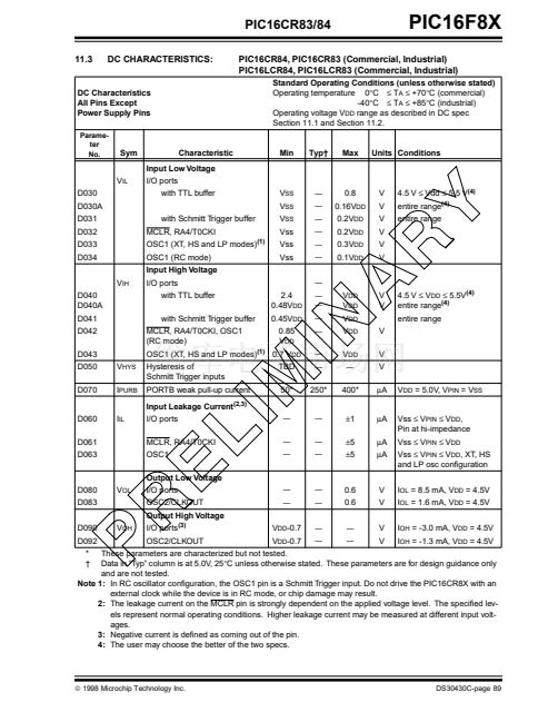
D092
OSC2/CLKOUT
V
DD
-0.7
V
I
OH
= -1.3 mA, V
DD
= 4.5V
*
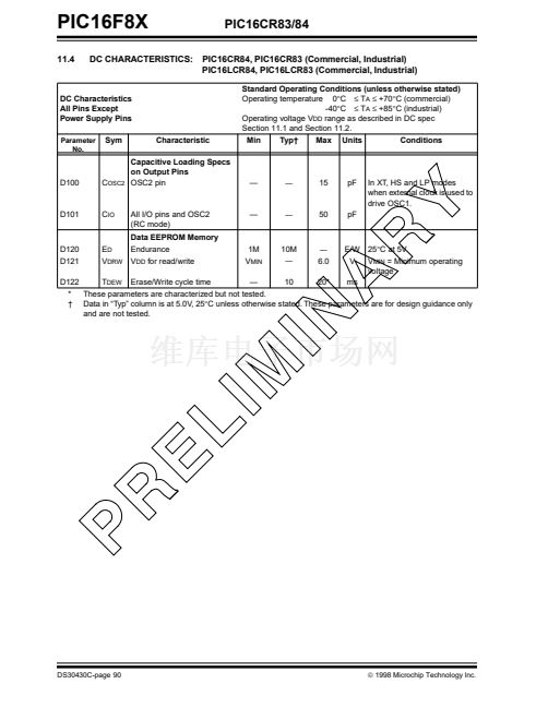
These parameters are characterized but not tested.
鈥?Data in 鈥淭yp鈥?column is at 5.0V, 25掳C unless otherwise stated. These parameters are for design guidance only
and are not tested.
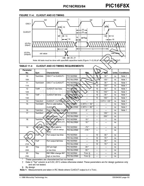
Note 1:
In RC oscillator con铿乬uration, the OSC1 pin is a Schmitt Trigger input. Do not drive the PIC16F8X with an
external clock while the device is in RC mode, or chip damage may result.
2:
The leakage current on the MCLR pin is strongly dependent on the applied voltage level. The speci铿乪d lev-
els represent normal operating conditions. Higher leakage current may be measured at different input volt-
ages.
3:
Negative current is de铿乶ed as coming out of the pin.
4:
The user may choose the better of the two specs.
漏
1998 Microchip Technology Inc.
DS30430C-page 77


 1
1
 2
2
 3
3
 4
4
 5
5
 6
6
 7
7
 8
8
 9
9
 10
10
 11
11
 12
12
 13
13
 14
14
 15
15
 16
16
 17
17
 18
18
 19
19
 20
20
 21
21
 22
22
 23
23
 24
24
 25
25
 26
26
 27
27
 28
28
 29
29
 30
30
 31
31
 32
32
 33
33
 34
34
 35
35
 36
36
 37
37
 38
38
 39
39
 40
40
 41
41
 42
42
 43
43
 44
44
 45
45
 46
46
 47
47
 48
48
 49
49
 50
50
 51
51
 52
52
 53
53
 54
54
 55
55
 56
56
 57
57
 58
58
 59
59
 60
60
 61
61
 62
62
 63
63
 64
64
 65
65
 66
66
 67
67
 68
68
 69
69
 70
70
 71
71
 72
72
 73
73
 74
74
 75
75
 76
76
 77
77
 78
78
 79
79
 80
80
 81
81
 82
82
 83
83
 84
84
 85
85
 86
86
 87
87
 88
88
 89
89
 90
90
 91
91
 92
92
 93
93
 94
94
 95
95
 96
96
 97
97
 98
98
 99
99
 100
100
 101
101
 102
102
 103
103
 104
104
 105
105
 106
106
 107
107
 108
108
 109
109
 110
110
 111
111
 112
112
 113
113
 114
114
 115
115
 116
116
 117
117
 118
118
 119
119
 120
120
 121
121
 122
122
 123
123
 124
124
