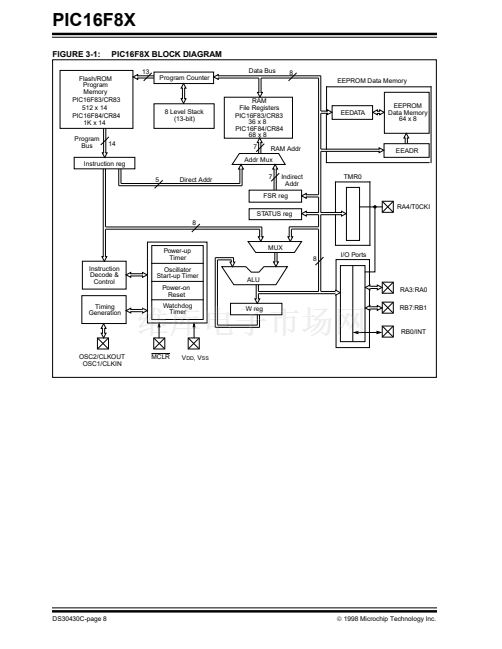
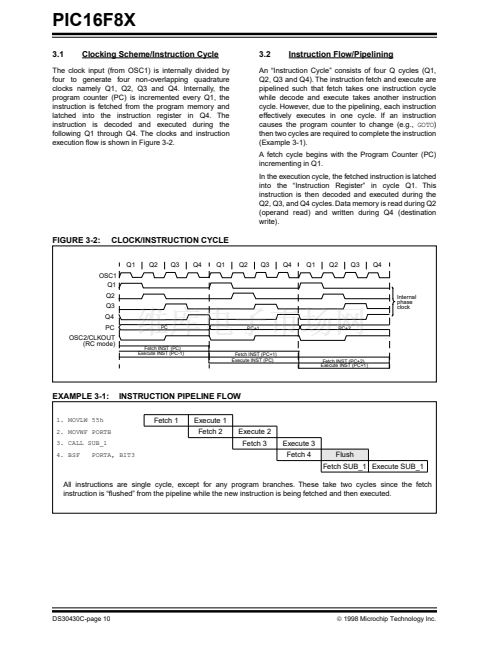
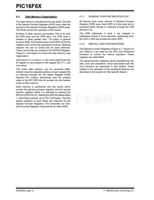
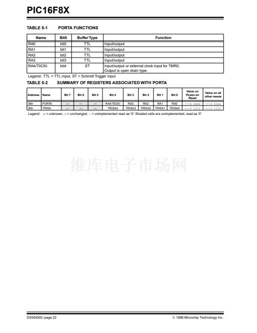
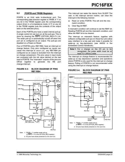
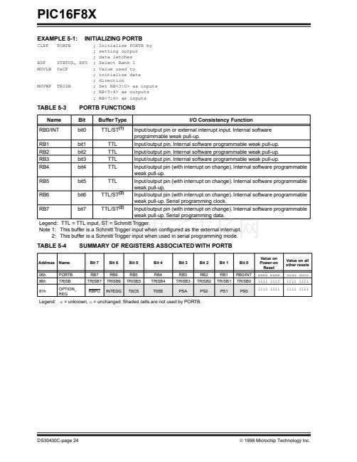
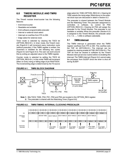
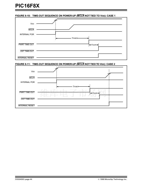
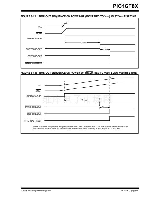
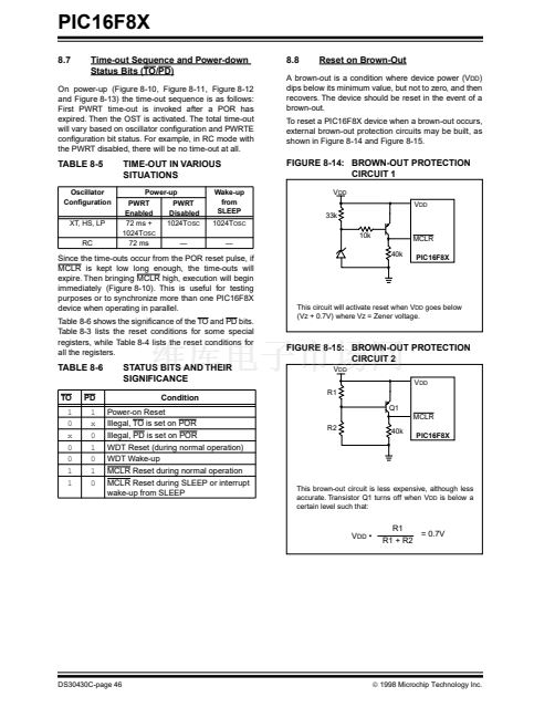
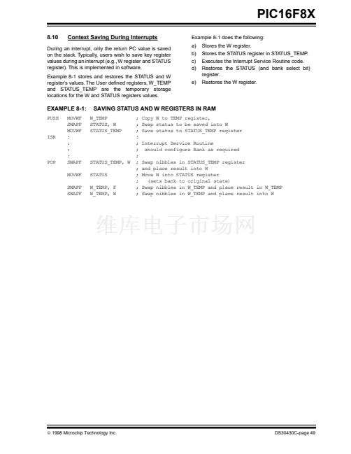
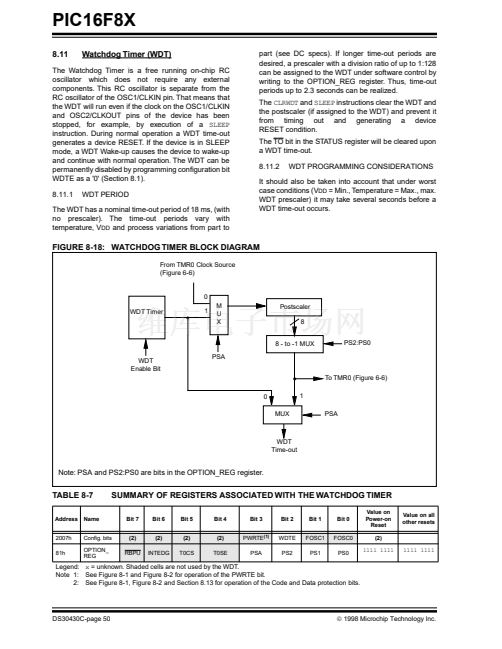
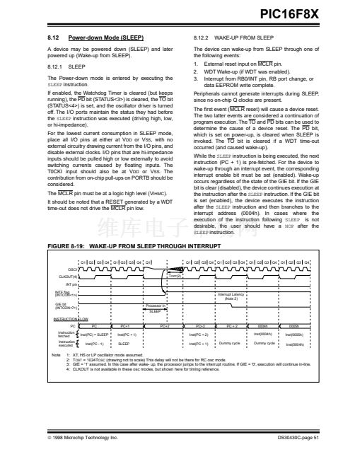
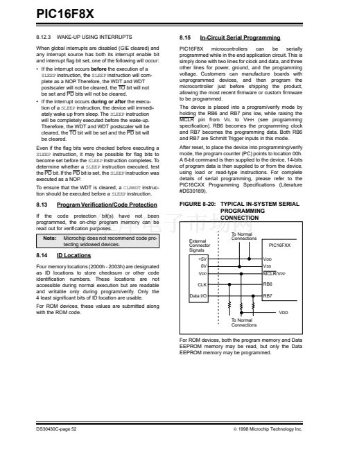
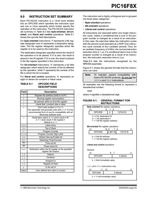
PIC16F8X
5.3
5.3.1
I/O Programming Considerations
BI-DIRECTIONAL I/O PORTS
5.3.2
SUCCESSIVE OPERATIONS ON I/O
PORTS
Any instruction which writes, operates internally as a
read followed by a write operation. The
BCF
and
BSF
instructions, for example, read the register into the
CPU, execute the bit operation and write the result back
to the register. Caution must be used when these
instructions are applied to a port with both inputs and
outputs de铿乶ed. For example, a
BSF
operation on bit5
of PORTB will cause all eight bits of PORTB to be read
into the CPU. Then the
BSF
operation takes place on
bit5 and PORTB is written to the output latches. If
another bit of PORTB is used as a bi-directional I/O pin
(i.e., bit0) and it is de铿乶ed as an input at this time, the
input signal present on the pin itself would be read into
the CPU and rewritten to the data latch of this particular
pin, overwriting the previous content. As long as the pin
stays in the input mode, no problem occurs. However,
if bit0 is switched into output mode later on, the content
of the data latch is unknown.
Reading the port register, reads the values of the port
pins. Writing to the port register writes the value to the
port latch. When using read-modify-write instructions
(i.e.,
BCF, BSF,
etc.) on a port, the value of the port pins
is read, the desired operation is done to this value, and
this value is then written to the port latch.
A pin actively outputting a Low or High should not be
driven from external devices at the same time in order
to change the level on this pin (鈥渨ired-or鈥? 鈥渨ired-and鈥?.
The resulting high output current may damage the chip.
The actual write to an I/O port happens at the end of an
instruction cycle, whereas for reading, the data must be
valid at the beginning of the instruction cycle
(Figure 5-5). Therefore, care must be exercised if a
write followed by a read operation is carried out on the
same I/O port. The sequence of instructions should be
such that the pin voltage stabilizes (load dependent)
before the next instruction which causes that 铿乴e to be
read into the CPU is executed. Otherwise, the previous
state of that pin may be read into the CPU rather than
the new state. When in doubt, it is better to separate
these instructions with a
NOP
or another instruction not
accessing this I/O port.
Example 5-1 shows the effect of two sequential
read-modify-write instructions (e.g.,
BCF, BSF,
etc.) on
an I/O port.
EXAMPLE 5-1:
READ-MODIFY-WRITE
INSTRUCTIONS ON AN
I/O PORT
;Initial PORT settings: PORTB<7:4> Inputs
;
PORTB<3:0> Outputs
;PORTB<7:6> have external pull-ups and are
;not connected to other circuitry
;
;
PORT latch PORT pins
;
---------- ---------
BCF PORTB, 7
; 01pp ppp
11pp ppp
BCF PORTB, 6
; 10pp ppp
11pp ppp
BSF STATUS, RP0 ;
BCF TRISB, 7
; 10pp ppp
11pp ppp
BCF TRISB, 6
; 10pp ppp
10pp ppp
;
;Note that the user may have expected the
;pin values to be 00pp ppp. The 2nd BCF
;caused RB7 to be latched as the pin value
;(high).
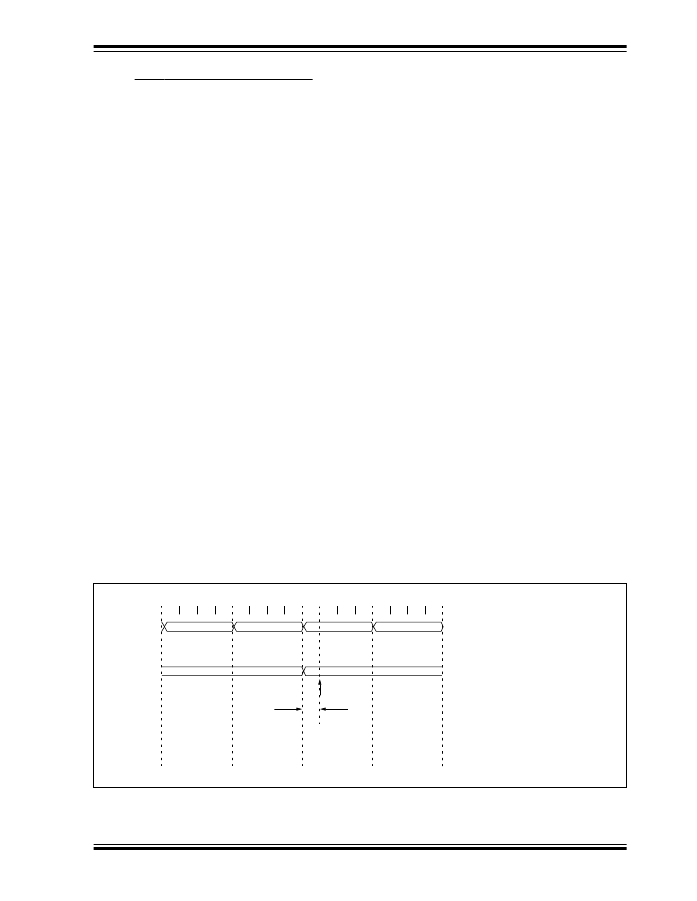
FIGURE 5-5:
SUCCESSIVE I/O OPERATION
Q1 Q2 Q3 Q4 Q1 Q2 Q3 Q4 Q1 Q2 Q3 Q4 Q1 Q2 Q3 Q4
Note:
This example shows a write to PORTB
followed by a read from PORTB.
Note that:
data setup time = (0.25T
CY
- T
PD
)
PC
Instruction
fetched
PC
PC + 1
PC + 2
NOP
PC + 3
NOP
MOVWF PORTB MOVF PORTB,W
write to
PORTB
RB7:RB0
Port pin
sampled here
Instruction
executed
MOVWF PORTB
write to
PORTB
T
PD
NOP
MOVF PORTB,W
where T
CY
= instruction cycle
T
PD
= propagation delay
Therefore, at higher clock frequencies,
a write followed by a read may be
problematic.
漏
1998 Microchip Technology Inc.
DS30430C-page 25


 1
1
 2
2
 3
3
 4
4
 5
5
 6
6
 7
7
 8
8
 9
9
 10
10
 11
11
 12
12
 13
13
 14
14
 15
15
 16
16
 17
17
 18
18
 19
19
 20
20
 21
21
 22
22
 23
23
 24
24
 25
25
 26
26
 27
27
 28
28
 29
29
 30
30
 31
31
 32
32
 33
33
 34
34
 35
35
 36
36
 37
37
 38
38
 39
39
 40
40
 41
41
 42
42
 43
43
 44
44
 45
45
 46
46
 47
47
 48
48
 49
49
 50
50
 51
51
 52
52
 53
53
 54
54
 55
55
 56
56
 57
57
 58
58
 59
59
 60
60
 61
61
 62
62
 63
63
 64
64
 65
65
 66
66
 67
67
 68
68
 69
69
 70
70
 71
71
 72
72
 73
73
 74
74
 75
75
 76
76
 77
77
 78
78
 79
79
 80
80
 81
81
 82
82
 83
83
 84
84
 85
85
 86
86
 87
87
 88
88
 89
89
 90
90
 91
91
 92
92
 93
93
 94
94
 95
95
 96
96
 97
97
 98
98
 99
99
 100
100
 101
101
 102
102
 103
103
 104
104
 105
105
 106
106
 107
107
 108
108
 109
109
 110
110
 111
111
 112
112
 113
113
 114
114
 115
115
 116
116
 117
117
 118
118
 119
119
 120
120
 121
121
 122
122
 123
123
 124
124
