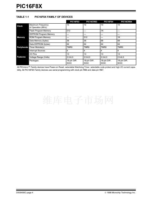
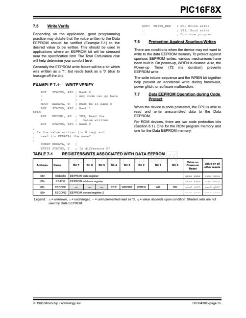
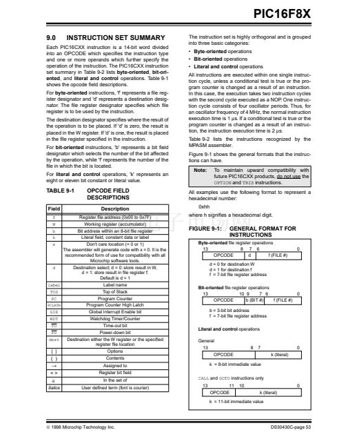
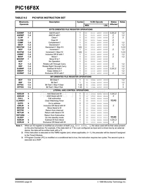
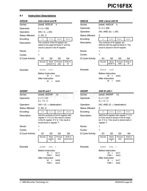
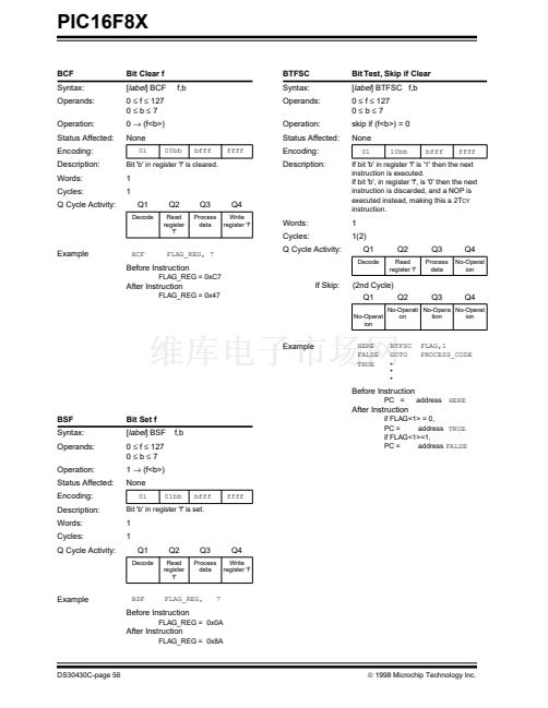
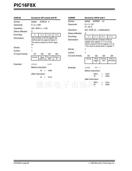
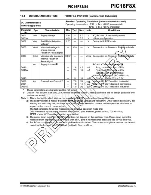
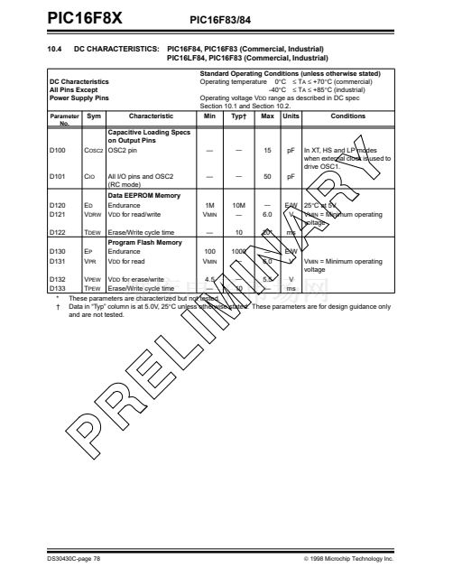
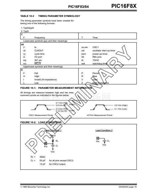
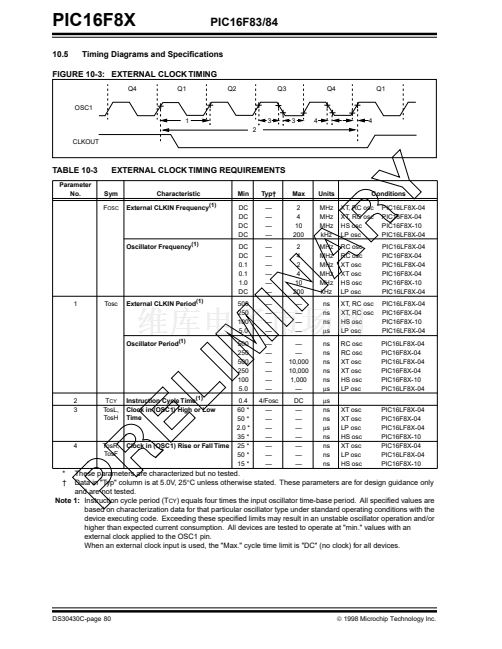
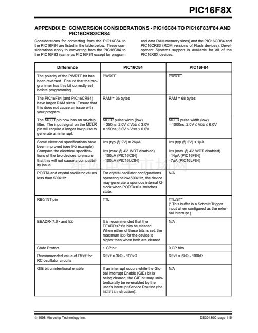
PIC16F8X
5.0
I/O PORTS
EXAMPLE 5-1:
CLRF
PORTA
INITIALIZING PORTA
;
;
;
;
;
;
;
;
;
;
;
Initialize PORTA by
setting output
data latches
Select Bank 1
Value used to
initialize data
direction
Set RA<3:0> as inputs
RA4 as outputs
TRISA<7:5> are always
read as '0'.
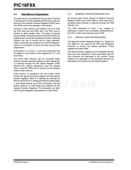
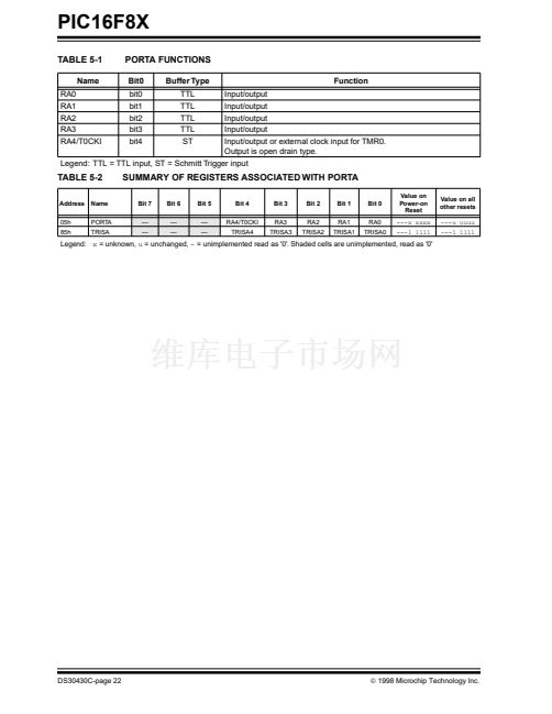
The PIC16F8X has two ports, PORTA and PORTB.
Some port pins are multiplexed with an alternate func-
tion for other features on the device.
5.1
PORTA and TRISA Registers
BSF
MOVLW
STATUS, RP0
0x0F
PORTA is a 5-bit wide latch. RA4 is a Schmitt Trigger
input and an open drain output. All other RA port pins
have TTL input levels and full CMOS output drivers. All
pins have data direction bits (TRIS registers) which can
con铿乬ure these pins as output or input.
Setting a TRISA bit (=1) will make the corresponding
PORTA pin an input, i.e., put the corresponding output
driver in a hi-impedance mode. Clearing a TRISA bit
(=0) will make the corresponding PORTA pin an output,
i.e., put the contents of the output latch on the selected
pin.
Reading the PORTA register reads the status of the pins
whereas writing to it will write to the port latch. All write
operations are read-modify-write operations. So a write
to a port implies that the port pins are 铿乺st read, then this
value is modi铿乪d and written to the port data latch.
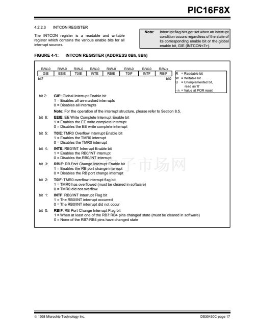
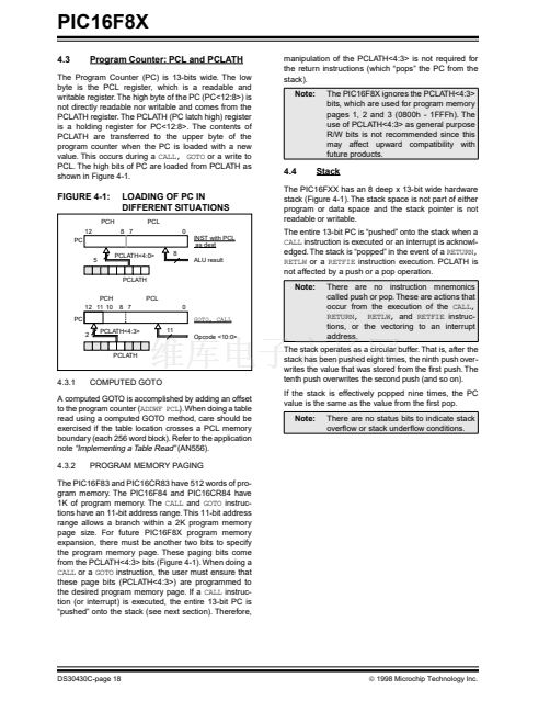
The RA4 pin is multiplexed with the TMR0 clock input.
MOVWF
TRISA
FIGURE 5-2:
Data
bus
WR
PORT
BLOCK DIAGRAM OF PIN RA4
D
Q
Q
CK
N
Data Latch
V
SS
D
Q
Q
RA4 pin
WR
TRIS
CK
TRIS Latch
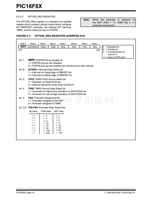
FIGURE 5-1:
Data
bus
D
WR
Port
BLOCK DIAGRAM OF PINS
RA3:RA0
RD TRIS
Q
V
DD
Q
Schmitt
Trigger
input
buffer
D
EN
EN
CK
Q
P
RD PORT
Data Latch
N
D
WR
TRIS
Q
V
SS
CK
Q
TTL
input
buffer
I/O pin
TMR0 clock input
Note: I/O pin has protection diodes to V
SS
only.
TRIS Latch
RD TRIS
Q
D
EN
RD PORT
Note: I/O pins have protection diodes to V
DD
and V
SS
.
漏
1998 Microchip Technology Inc.
DS30430C-page 21


 1
1
 2
2
 3
3
 4
4
 5
5
 6
6
 7
7
 8
8
 9
9
 10
10
 11
11
 12
12
 13
13
 14
14
 15
15
 16
16
 17
17
 18
18
 19
19
 20
20
 21
21
 22
22
 23
23
 24
24
 25
25
 26
26
 27
27
 28
28
 29
29
 30
30
 31
31
 32
32
 33
33
 34
34
 35
35
 36
36
 37
37
 38
38
 39
39
 40
40
 41
41
 42
42
 43
43
 44
44
 45
45
 46
46
 47
47
 48
48
 49
49
 50
50
 51
51
 52
52
 53
53
 54
54
 55
55
 56
56
 57
57
 58
58
 59
59
 60
60
 61
61
 62
62
 63
63
 64
64
 65
65
 66
66
 67
67
 68
68
 69
69
 70
70
 71
71
 72
72
 73
73
 74
74
 75
75
 76
76
 77
77
 78
78
 79
79
 80
80
 81
81
 82
82
 83
83
 84
84
 85
85
 86
86
 87
87
 88
88
 89
89
 90
90
 91
91
 92
92
 93
93
 94
94
 95
95
 96
96
 97
97
 98
98
 99
99
 100
100
 101
101
 102
102
 103
103
 104
104
 105
105
 106
106
 107
107
 108
108
 109
109
 110
110
 111
111
 112
112
 113
113
 114
114
 115
115
 116
116
 117
117
 118
118
 119
119
 120
120
 121
121
 122
122
 123
123
 124
124
