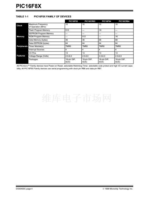
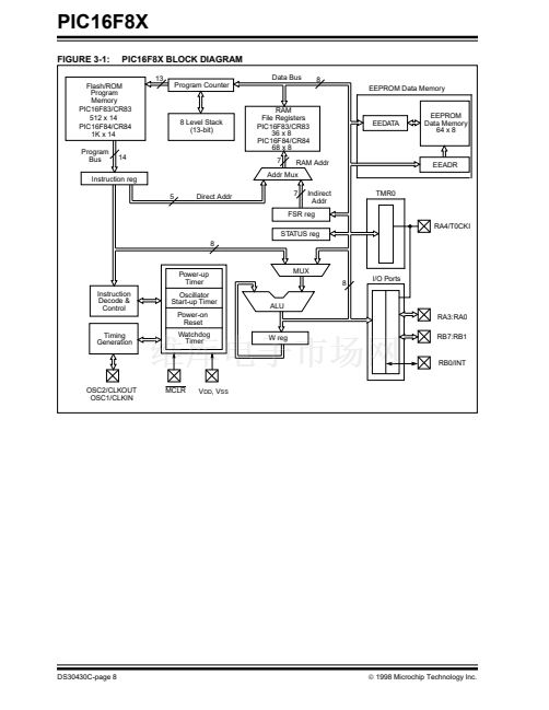
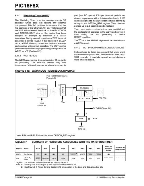
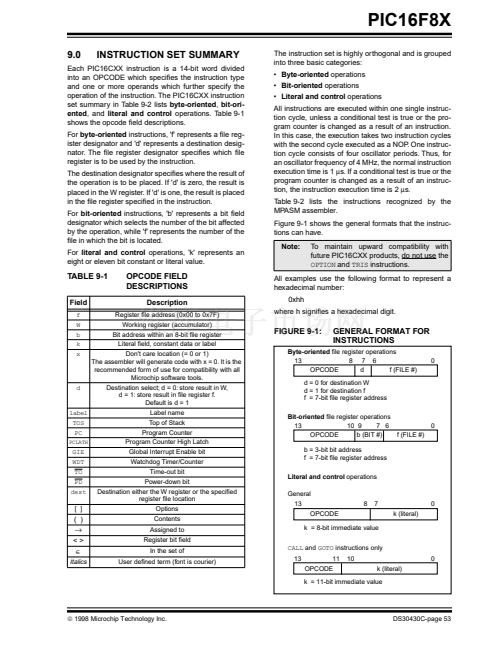
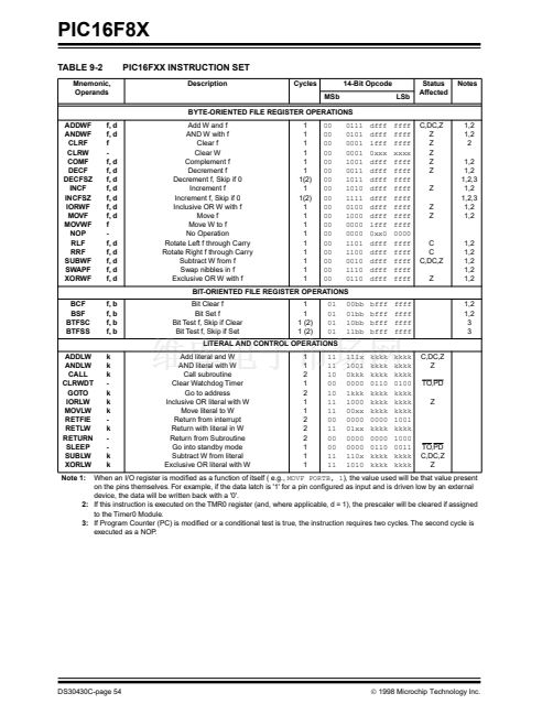
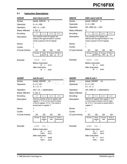
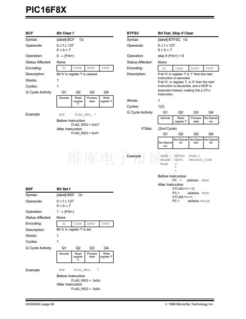
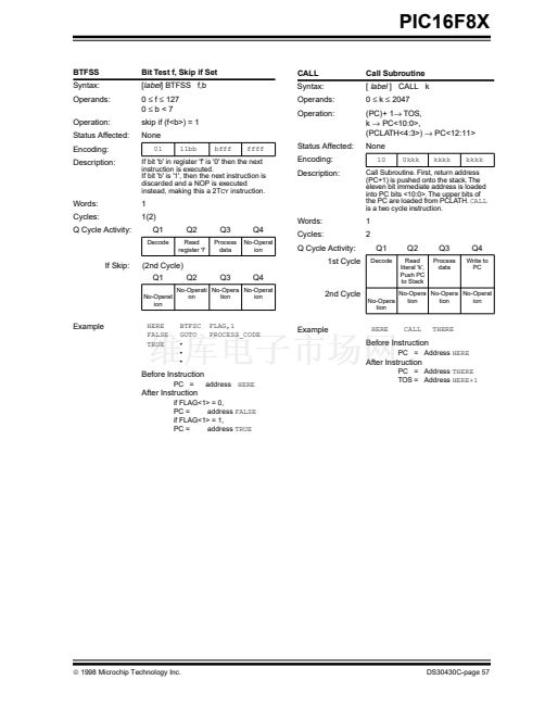
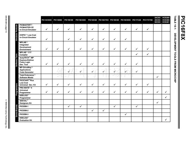
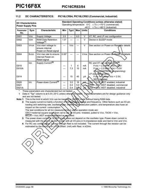
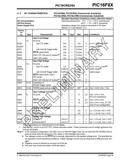
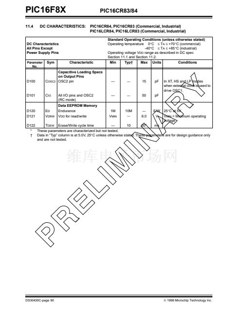
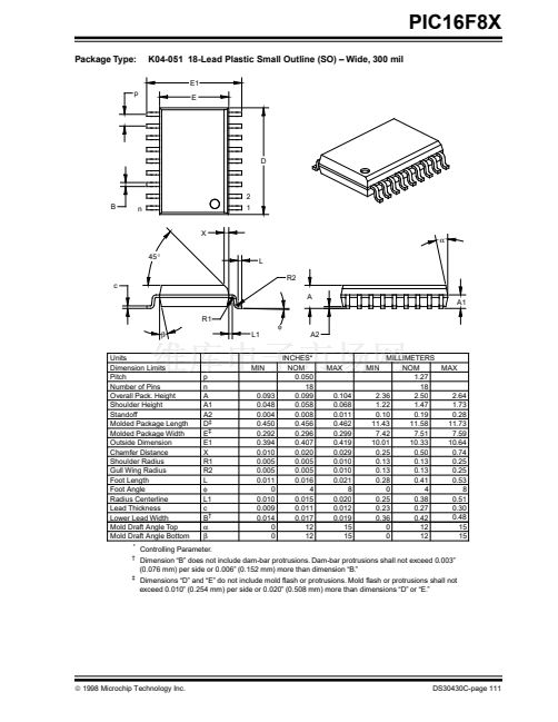
PIC16F8X
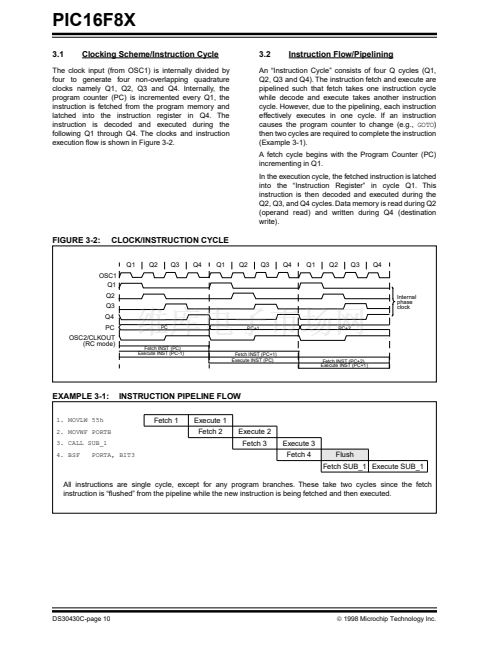
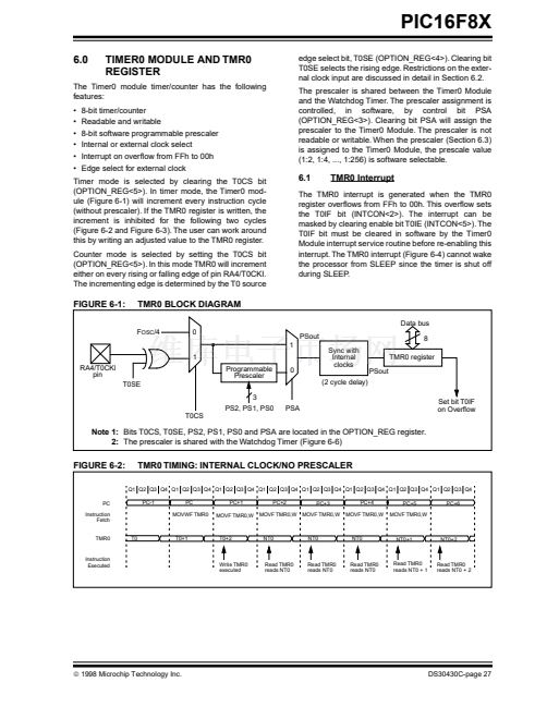
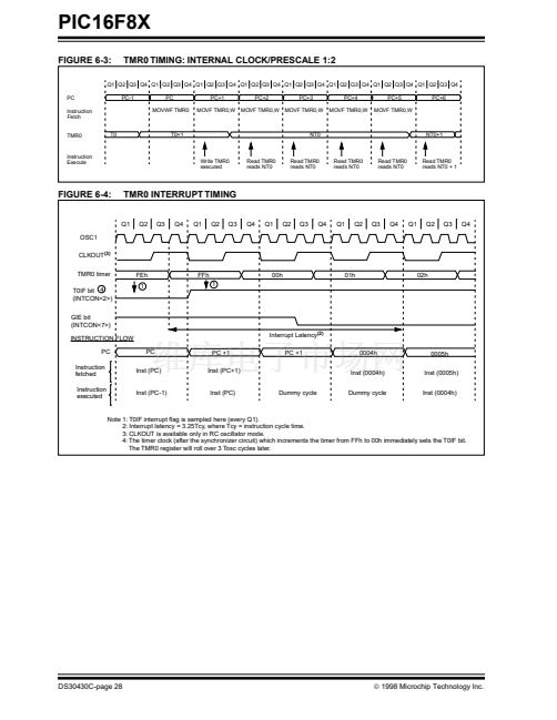
FIGURE 6-3:
TMR0 TIMING: INTERNAL CLOCK/PRESCALE 1:2
Q1 Q2 Q3 Q4 Q1 Q2 Q3 Q4 Q1 Q2 Q3 Q4 Q1 Q2 Q3 Q4 Q1 Q2 Q3 Q4 Q1 Q2 Q3 Q4 Q1 Q2 Q3 Q4 Q1 Q2 Q3 Q4
PC
Instruction
Fetch
TMR0
T0
PC-1
PC
MOVWF TMR0
PC+1
MOVF TMR0,W
PC+2
MOVF TMR0,W
PC+3
MOVF TMR0,W
PC+4
MOVF TMR0,W
PC+5
MOVF TMR0,W
PC+6
T0+1
NT0
NT0+1
Instruction
Execute
Write TMR0
executed
Read TMR0
reads NT0
Read TMR0
reads NT0
Read TMR0
reads NT0
Read TMR0
reads NT0
Read TMR0
reads NT0 + 1
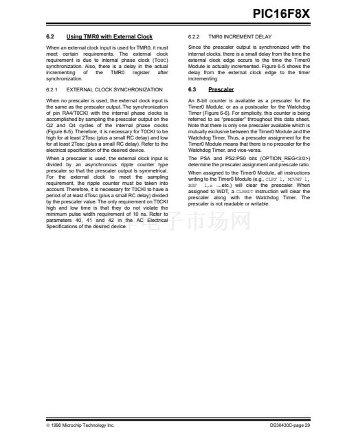
FIGURE 6-4:
TMR0 INTERRUPT TIMING
Q1
Q2
Q3
Q4
Q1
Q2
Q3
Q4
Q1
Q2
Q3
Q4
Q1
Q2
Q3
Q4
Q1
Q2
Q3
Q4
OSC1
CLKOUT
(3)
TMR0 timer
T0IF bit 4
(INTCON<2>)
GIE bit
(INTCON<7>)
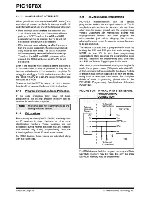
INSTRUCTION FLOW
PC
Instruction
fetched
Instruction
executed
PC
Inst (PC)
Inst (PC-1)
PC +1
Inst (PC+1)
Dummy cycle
Interrupt Latency
(2)
PC +1
0004h
Inst (0004h)
Dummy cycle
0005h
Inst (0005h)
Inst (0004h)
FEh
1
FFh
1
00h
01h
02h
Inst (PC)
Note 1: T0IF interrupt 铿俛g is sampled here (every Q1).
2: Interrupt latency = 3.25Tcy, where Tcy = instruction cycle time.
3: CLKOUT is available only in RC oscillator mode.
4: The timer clock (after the synchronizer circuit) which increments the timer from FFh to 00h immediately sets the T0IF bit.
The TMR0 register will roll over 3 Tosc cycles later.
DS30430C-page 28
漏
1998 Microchip Technology Inc.


 1
1
 2
2
 3
3
 4
4
 5
5
 6
6
 7
7
 8
8
 9
9
 10
10
 11
11
 12
12
 13
13
 14
14
 15
15
 16
16
 17
17
 18
18
 19
19
 20
20
 21
21
 22
22
 23
23
 24
24
 25
25
 26
26
 27
27
 28
28
 29
29
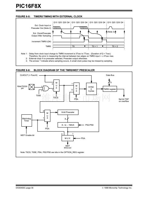 30
30
 31
31
 32
32
 33
33
 34
34
 35
35
 36
36
 37
37
 38
38
 39
39
 40
40
 41
41
 42
42
 43
43
 44
44
 45
45
 46
46
 47
47
 48
48
 49
49
 50
50
 51
51
 52
52
 53
53
 54
54
 55
55
 56
56
 57
57
 58
58
 59
59
 60
60
 61
61
 62
62
 63
63
 64
64
 65
65
 66
66
 67
67
 68
68
 69
69
 70
70
 71
71
 72
72
 73
73
 74
74
 75
75
 76
76
 77
77
 78
78
 79
79
 80
80
 81
81
 82
82
 83
83
 84
84
 85
85
 86
86
 87
87
 88
88
 89
89
 90
90
 91
91
 92
92
 93
93
 94
94
 95
95
 96
96
 97
97
 98
98
 99
99
 100
100
 101
101
 102
102
 103
103
 104
104
 105
105
 106
106
 107
107
 108
108
 109
109
 110
110
 111
111
 112
112
 113
113
 114
114
 115
115
 116
116
 117
117
 118
118
 119
119
 120
120
 121
121
 122
122
 123
123
 124
124
