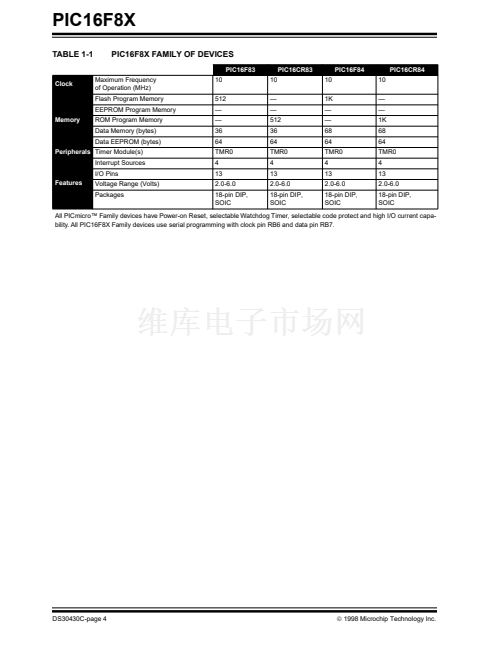
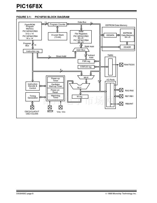
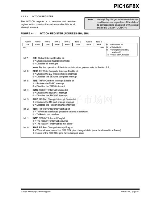
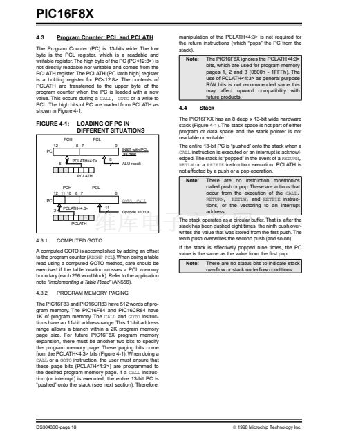
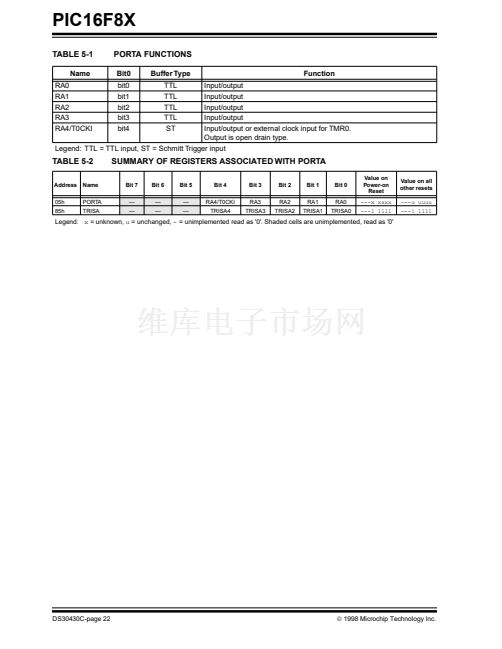
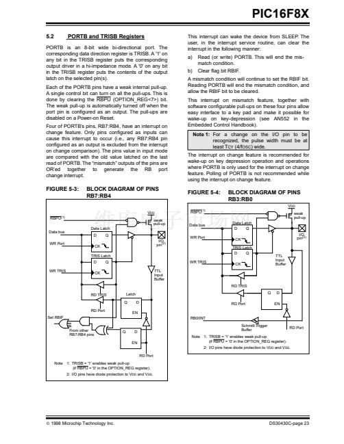
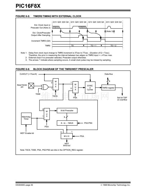
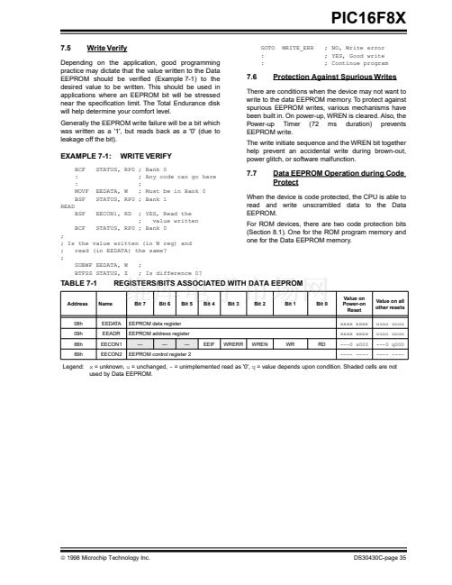
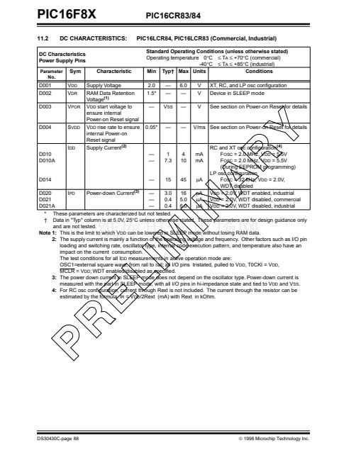
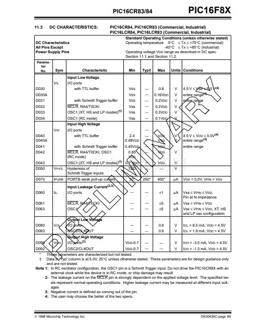
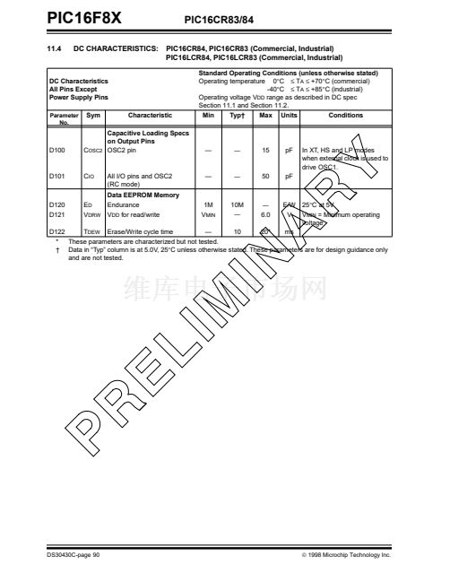
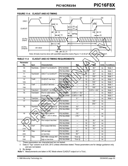
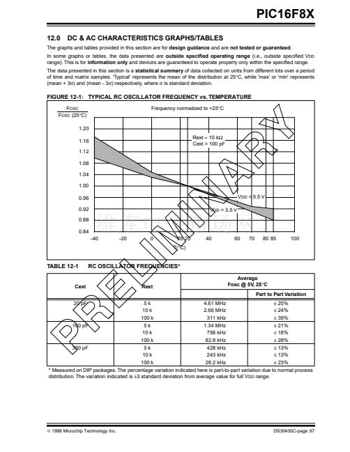
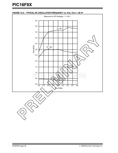
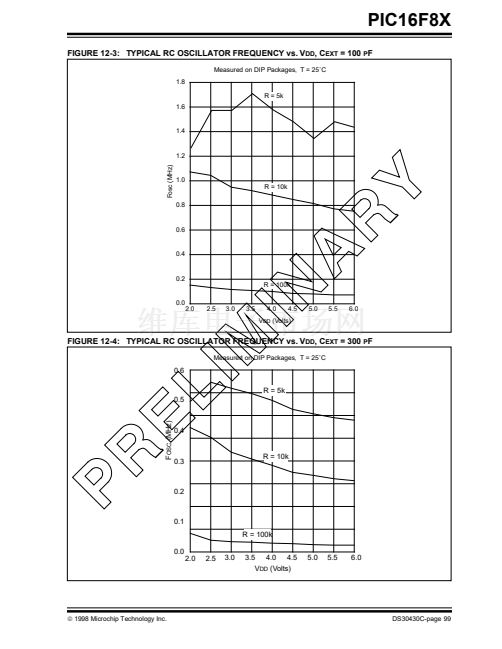
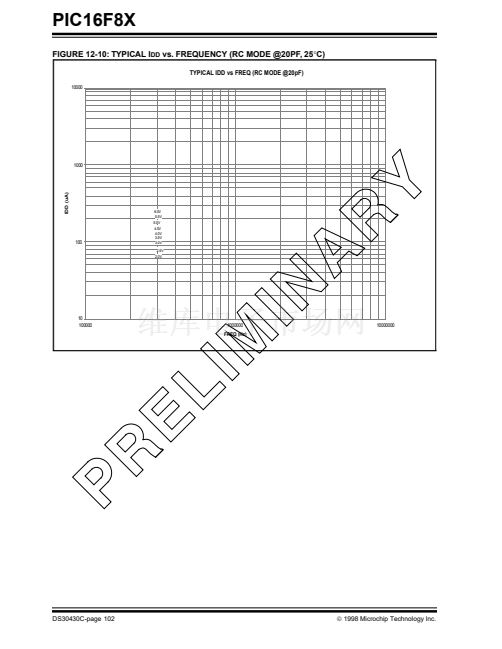
PIC16F8X
8.12.3
WAKE-UP USING INTERRUPTS
8.15
In-Circuit Serial Programming
When global interrupts are disabled (GIE cleared) and
any interrupt source has both its interrupt enable bit
and interrupt 铿俛g bit set, one of the following will occur:
鈥?If the interrupt occurs
before
the execution of a
SLEEP
instruction, the
SLEEP
instruction will com-
plete as a NOP. Therefore, the WDT and WDT
postscaler will not be cleared, the TO bit will not
be set and PD bits will not be cleared.
鈥?If the interrupt occurs
during or after
the execu-
tion of a
SLEEP
instruction, the device will immedi-
ately wake up from sleep. The
SLEEP
instruction
will be completely executed before the wake-up.
Therefore, the WDT and WDT postscaler will be
cleared, the TO bit will be set and the PD bit will
be cleared.
Even if the 铿俛g bits were checked before executing a
SLEEP
instruction, it may be possible for flag bits to
become set before the
SLEEP
instruction completes. To
determine whether a
SLEEP
instruction executed, test
the PD bit. If the PD bit is set, the
SLEEP
instruction was
executed as a NOP.
To ensure that the WDT is cleared, a
CLRWDT
instruc-
tion should be executed before a
SLEEP
instruction.
PIC16F8X
microcontrollers
can
be
serially
programmed while in the end application circuit. This is
simply done with two lines for clock and data, and three
other lines for power, ground, and the programming
voltage. Customers can manufacture boards with
unprogrammed devices, and then program the
microcontroller just before shipping the product,
allowing the most recent 铿乺mware or custom 铿乺mware
to be programmed.
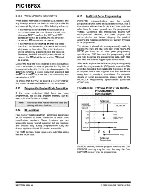
The device is placed into a program/verify mode by
holding the RB6 and RB7 pins low, while raising the
MCLR pin from V
IL
to V
IHH
(see programming
speci铿乧ation). RB6 becomes the programming clock
and RB7 becomes the programming data. Both RB6
and RB7 are Schmitt Trigger inputs in this mode.
After reset, to place the device into programming/verify
mode, the program counter (PC) points to location 00h.
A 6-bit command is then supplied to the device, 14-bits
of program data is then supplied to or from the device,
using load or read-type instructions. For complete
details of serial programming, please refer to the
PIC16CXX Programming Speci铿乧ations (Literature
#DS30189).
8.13
Program Veri铿乧ation/Code Protection
If the code protection bit(s) have not been
programmed, the on-chip program memory can be
read out for veri铿乧ation purposes.
Note:
Microchip does not recommend code pro-
tecting widowed devices.
FIGURE 8-20: TYPICAL IN-SYSTEM SERIAL
PROGRAMMING
CONNECTION
To Normal
Connections
PIC16FXX
V
DD
V
SS
MCLR/V
PP
RB6
RB7
External
Connector
Signals
+5V
0V
V
PP
CLK
Data I/O
8.14
ID Locations
Four memory locations (2000h - 2003h) are designated
as ID locations to store checksum or other code
identi铿乧ation numbers. These locations are not
accessible during normal execution but are readable
and writable only during program/verify. Only the
4 least signi铿乧ant bits of ID location are usable.
For ROM devices, these values are submitted along
with the ROM code.
V
DD
To Normal
Connections
For ROM devices, both the program memory and Data
EEPROM memory may be read, but only the Data
EEPROM memory may be programmed.
DS30430C-page 52
漏
1998 Microchip Technology Inc.


 1
1
 2
2
 3
3
 4
4
 5
5
 6
6
 7
7
 8
8
 9
9
 10
10
 11
11
 12
12
 13
13
 14
14
 15
15
 16
16
 17
17
 18
18
 19
19
 20
20
 21
21
 22
22
 23
23
 24
24
 25
25
 26
26
 27
27
 28
28
 29
29
 30
30
 31
31
 32
32
 33
33
 34
34
 35
35
 36
36
 37
37
 38
38
 39
39
 40
40
 41
41
 42
42
 43
43
 44
44
 45
45
 46
46
 47
47
 48
48
 49
49
 50
50
 51
51
 52
52
 53
53
 54
54
 55
55
 56
56
 57
57
 58
58
 59
59
 60
60
 61
61
 62
62
 63
63
 64
64
 65
65
 66
66
 67
67
 68
68
 69
69
 70
70
 71
71
 72
72
 73
73
 74
74
 75
75
 76
76
 77
77
 78
78
 79
79
 80
80
 81
81
 82
82
 83
83
 84
84
 85
85
 86
86
 87
87
 88
88
 89
89
 90
90
 91
91
 92
92
 93
93
 94
94
 95
95
 96
96
 97
97
 98
98
 99
99
 100
100
 101
101
 102
102
 103
103
 104
104
 105
105
 106
106
 107
107
 108
108
 109
109
 110
110
 111
111
 112
112
 113
113
 114
114
 115
115
 116
116
 117
117
 118
118
 119
119
 120
120
 121
121
 122
122
 123
123
 124
124
