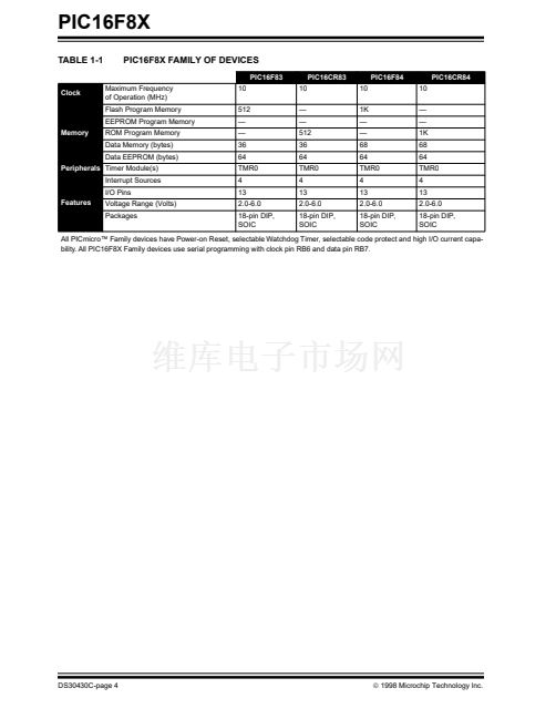
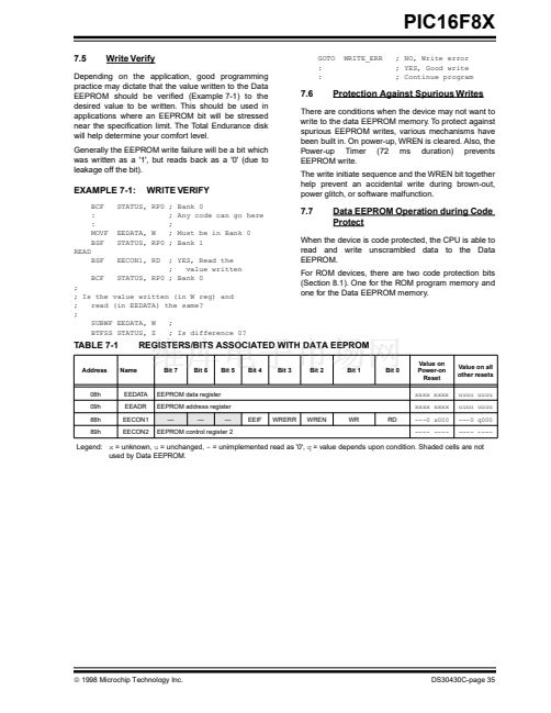
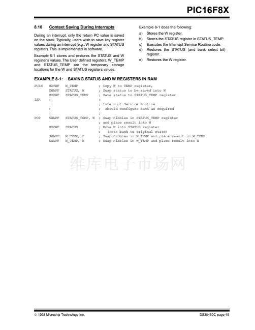
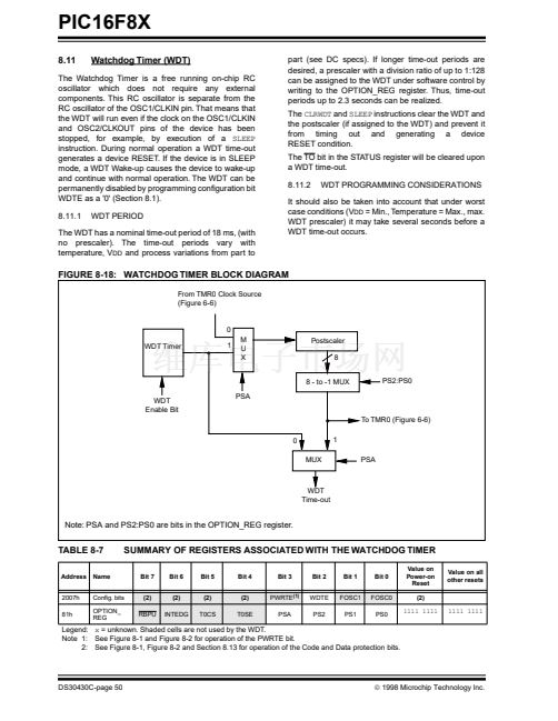
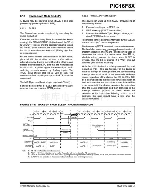
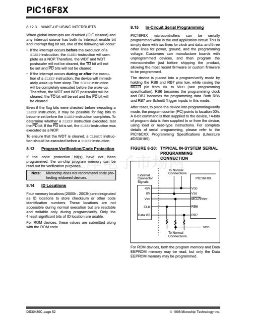
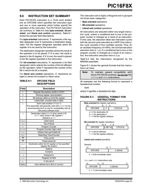
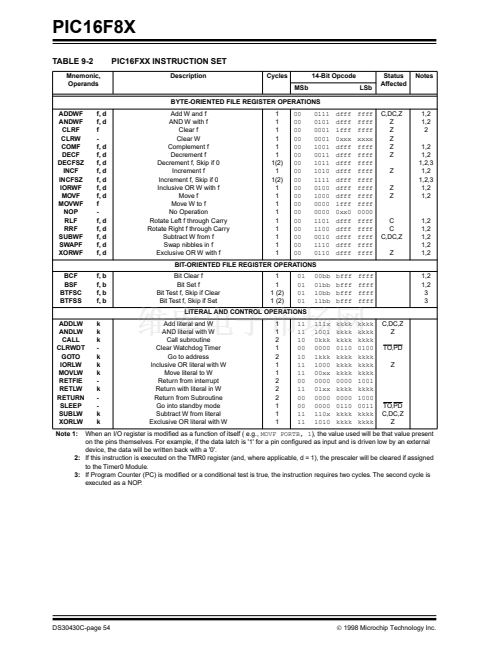
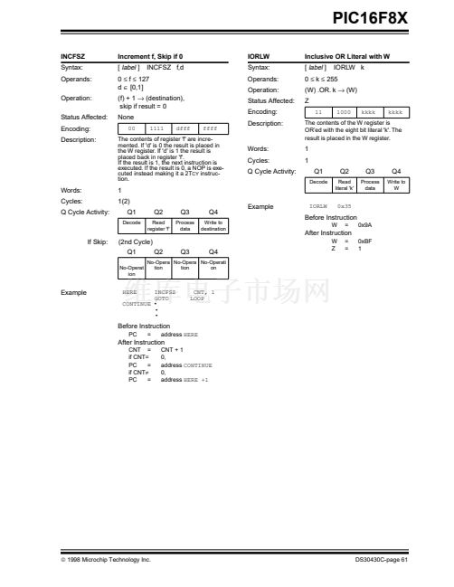
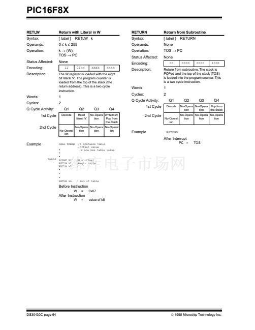
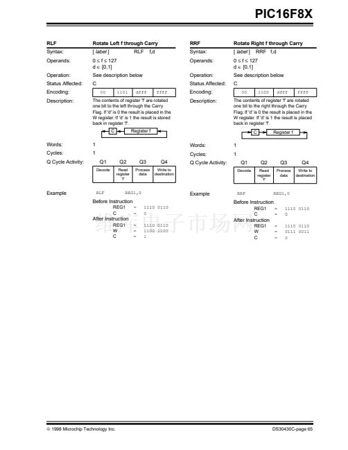
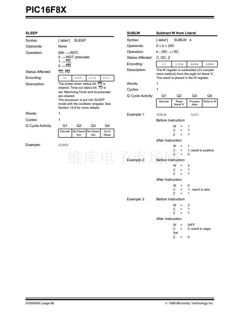
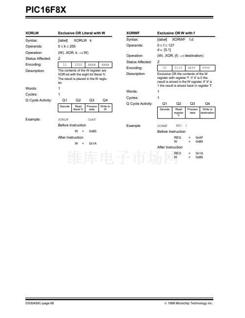
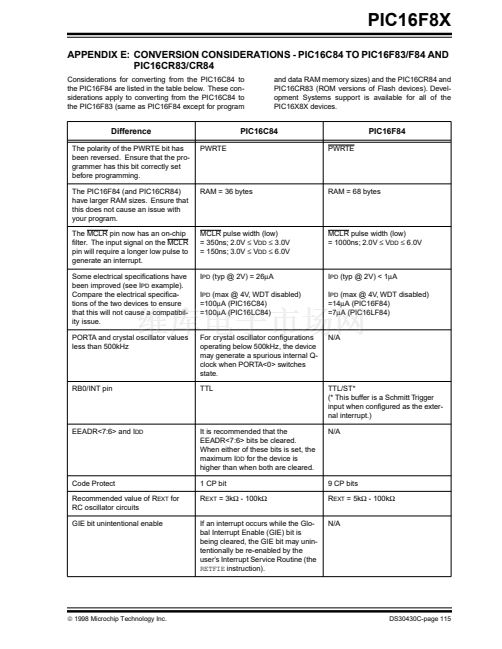
PIC16F83/84
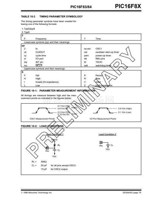
TABLE 10-2
TIMING PARAMETER SYMBOLOGY
PIC16F8X
The timing parameter symbols have been created fol-
lowing one of the following formats:
1. TppS2ppS
2. TppS
T
F
Frequency
Lowercase symbols (pp) and their meanings:
pp
2
to
ck
CLKOUT
cy
cycle time
io
I/O port
inp
INT pin
mc
MCLR
Uppercase symbols and their meanings:
S
F
Fall
H
High
I
Invalid (Hi-impedance)
L
Low
T
Time
os,osc
ost
pwrt
rbt
t0
wdt
OSC1
oscillator start-up timer
power-up timer
RBx pins
T0CKI
watchdog timer
P
R
V
Z
Period
Rise
Valid
High Impedance
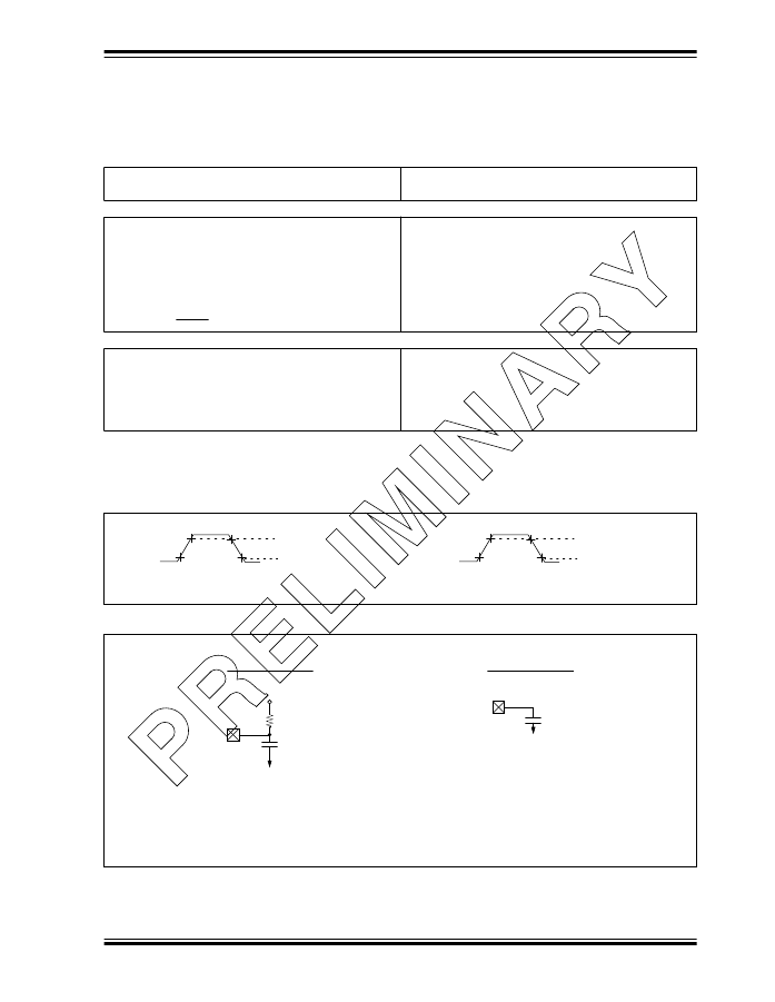
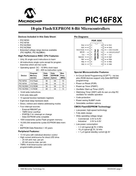
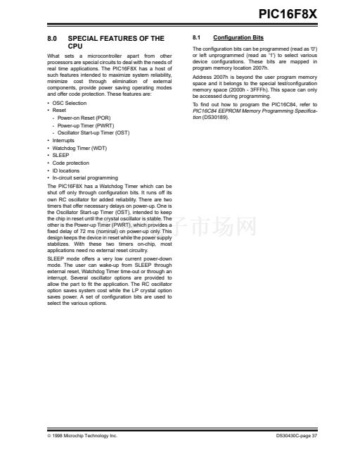
FIGURE 10-1: PARAMETER MEASUREMENT INFORMATION
All timings are measure between high and low mea-
surement points as indicated in the 铿乬ures below.
0.7 V
DD
XTAL
0.8 V
DD
RC (High)
0.3 V
DD
XTAL
0.15 V
DD
RC (Low)
OSC1 Measurement Points
I/O Port Measurement Points
0.9 V
DD
(High)
0.1 V
DD
(Low)
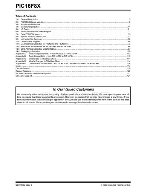
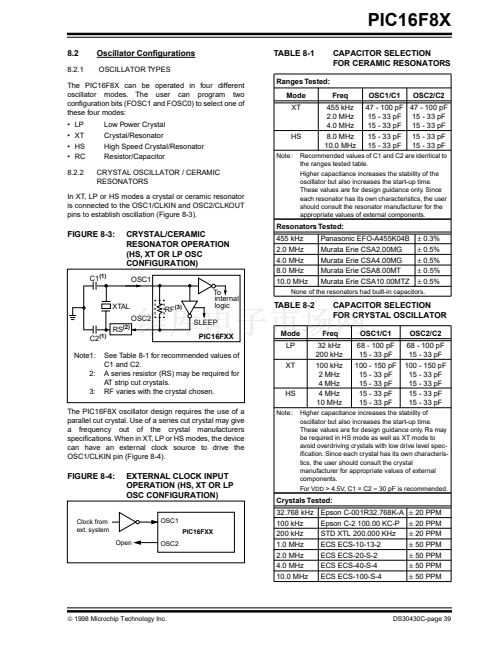
FIGURE 10-2: LOAD CONDITIONS
Load Condition 1
V
DD
/2
R
L
Pin
V
SS
R
L
=
C
L
=
464鈩?/div>
50 pF
15 pF
for all pins except OSC2.
for OSC2 output.
C
L
Pin
V
SS
C
L
Load Condition 2
漏
1998 Microchip Technology Inc.
DS30430C-page 79


 1
1
 2
2
 3
3
 4
4
 5
5
 6
6
 7
7
 8
8
 9
9
 10
10
 11
11
 12
12
 13
13
 14
14
 15
15
 16
16
 17
17
 18
18
 19
19
 20
20
 21
21
 22
22
 23
23
 24
24
 25
25
 26
26
 27
27
 28
28
 29
29
 30
30
 31
31
 32
32
 33
33
 34
34
 35
35
 36
36
 37
37
 38
38
 39
39
 40
40
 41
41
 42
42
 43
43
 44
44
 45
45
 46
46
 47
47
 48
48
 49
49
 50
50
 51
51
 52
52
 53
53
 54
54
 55
55
 56
56
 57
57
 58
58
 59
59
 60
60
 61
61
 62
62
 63
63
 64
64
 65
65
 66
66
 67
67
 68
68
 69
69
 70
70
 71
71
 72
72
 73
73
 74
74
 75
75
 76
76
 77
77
 78
78
 79
79
 80
80
 81
81
 82
82
 83
83
 84
84
 85
85
 86
86
 87
87
 88
88
 89
89
 90
90
 91
91
 92
92
 93
93
 94
94
 95
95
 96
96
 97
97
 98
98
 99
99
 100
100
 101
101
 102
102
 103
103
 104
104
 105
105
 106
106
 107
107
 108
108
 109
109
 110
110
 111
111
 112
112
 113
113
 114
114
 115
115
 116
116
 117
117
 118
118
 119
119
 120
120
 121
121
 122
122
 123
123
 124
124
