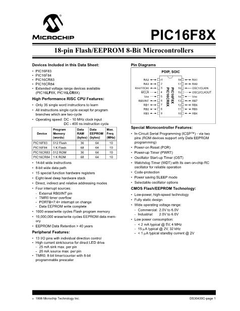
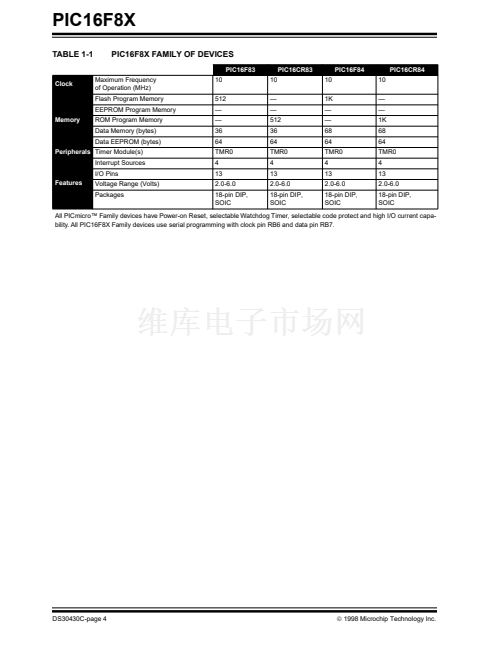
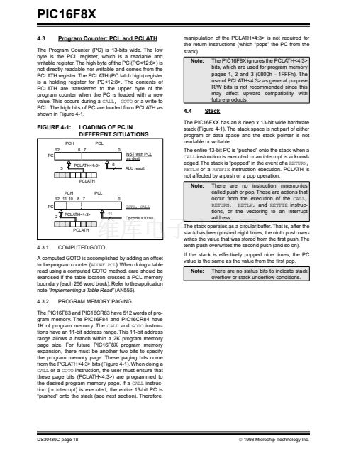
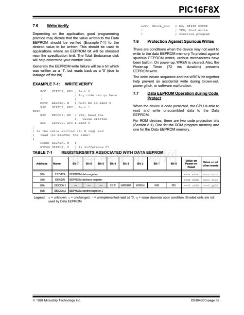
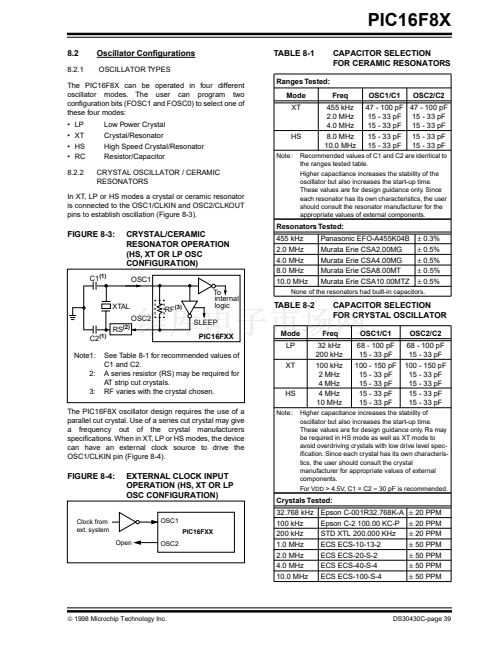
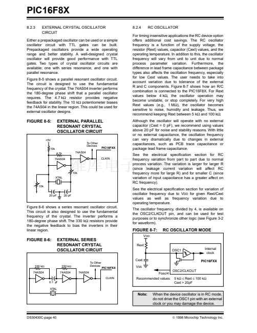
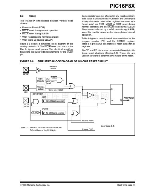
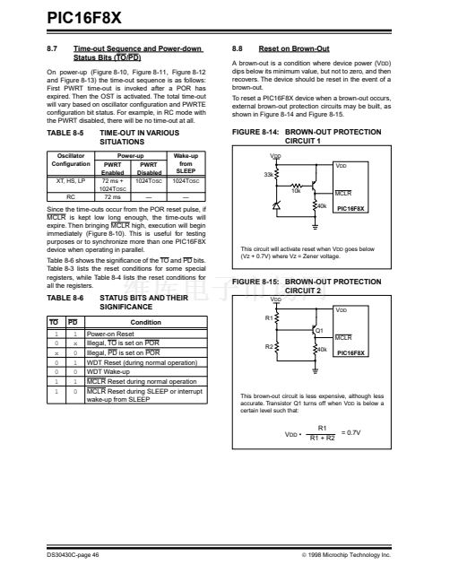
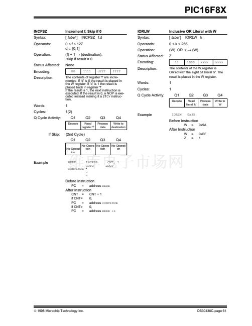
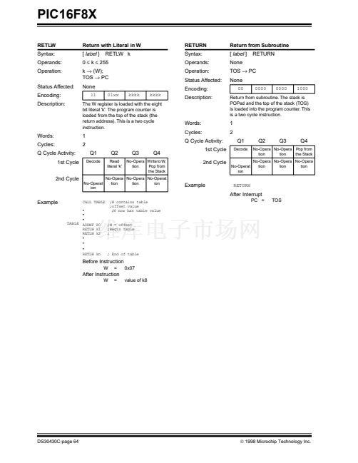
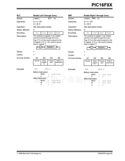
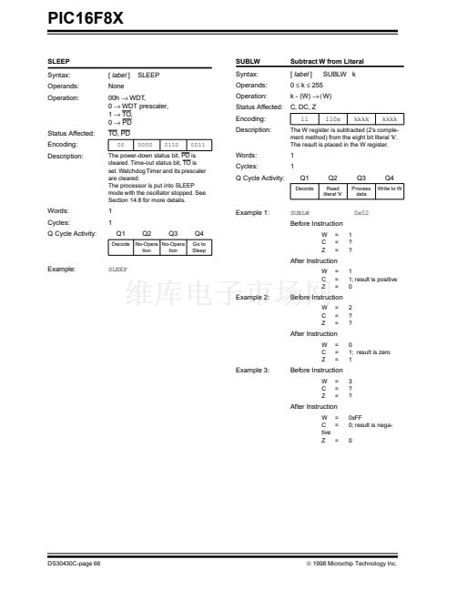
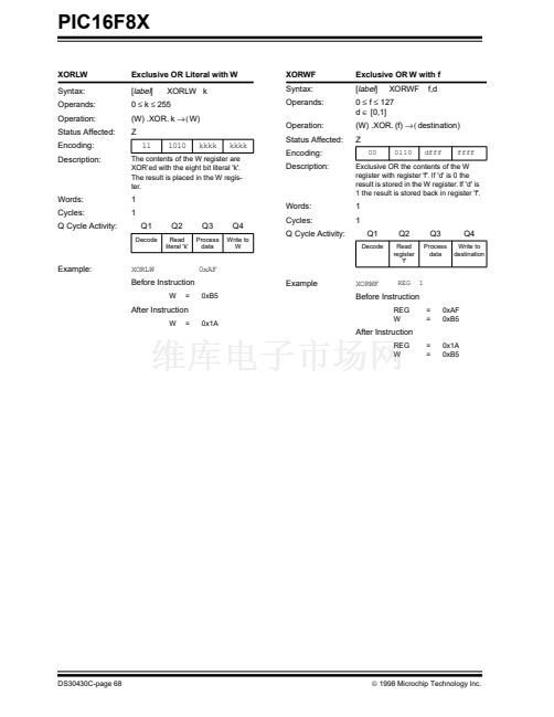
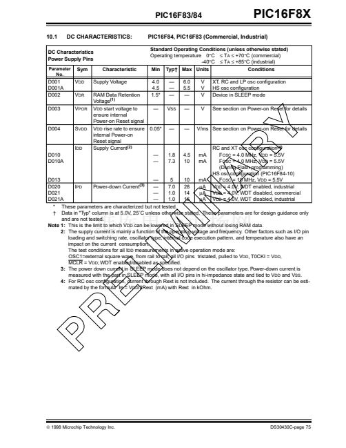
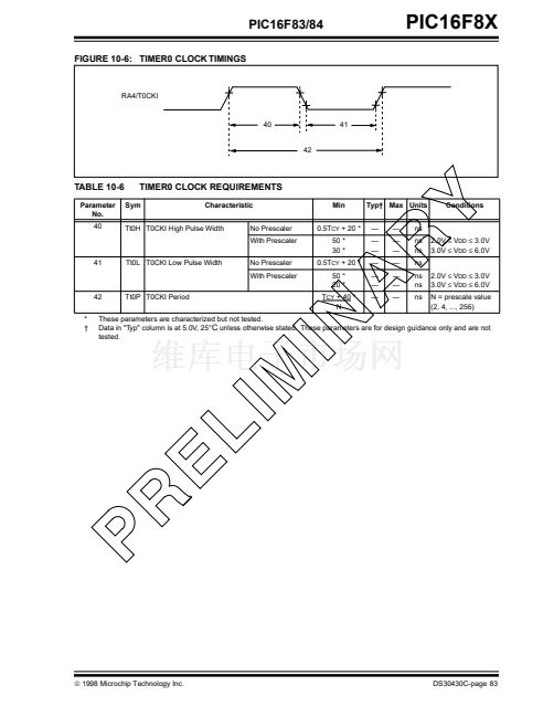
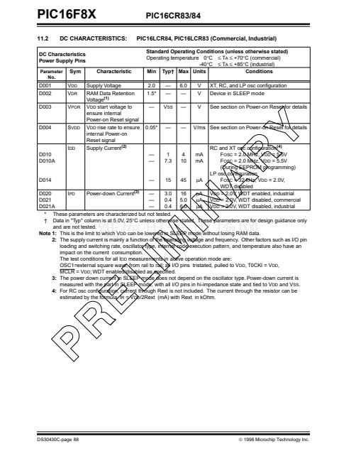
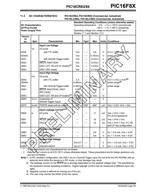
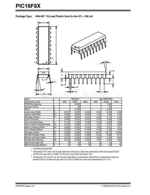
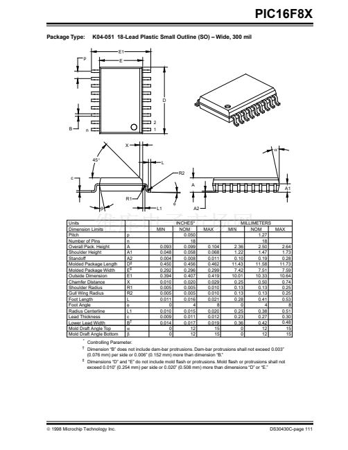
PIC16F8X
8.4
Power-on Reset (POR)
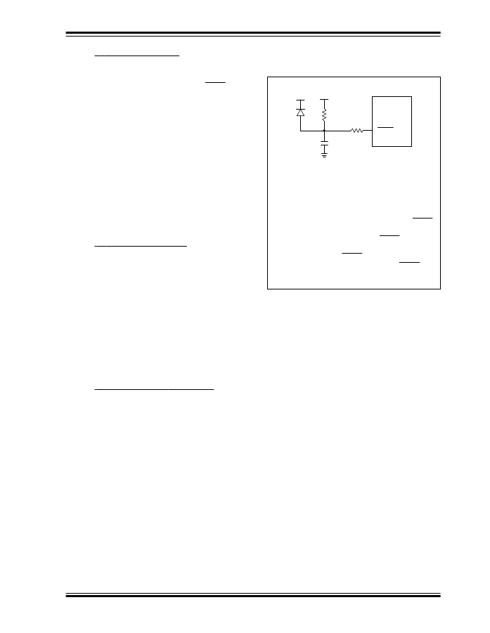
FIGURE 8-9:
A Power-on Reset pulse is generated on-chip when
V
DD
rise is detected (in the range of 1.2V - 1.7V). To
take advantage of the POR, just tie the MCLR pin
directly (or through a resistor) to V
DD
. This will eliminate
external RC components usually needed to create
Power-on Reset. A minimum rise time for V
DD
must be
met for this to operate properly. See Electrical Speci铿?
cations for details.
When the device starts normal operation (exits the
reset condition), device operating parameters (voltage,
frequency, temperature, ...) must be meet to ensure
operation. If these conditions are not met, the device
must be held in reset until the operating conditions
are met.
For additional information, refer to Application Note
AN607, "Power-up
Trouble Shooting."
The POR circuit does not produce an internal reset
when V
DD
declines.
EXTERNAL POWER-ON
RESET CIRCUIT (FOR SLOW
V
DD
POWER-UP)
V
DD
V
DD
D
R
R1
MCLR
C
PIC16FXX
8.5
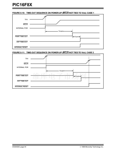
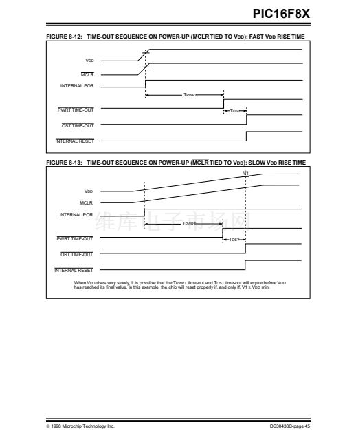
Power-up Timer (PWRT)
The Power-up Timer (PWRT) provides a 铿亁ed 72 ms
nominal time-out (T
PWRT
) from POR (Figure 8-10,
Figure 8-11, Figure 8-12 and Figure 8-13). The
Power-up Timer operates on an internal RC oscillator.
The chip is kept in reset as long as the PWRT is active.
The PWRT delay allows the V
DD
to rise to an accept-
able level (Possible exception shown in Figure 8-13).
A con铿乬uration bit, PWRTE, can enable/disable the
PWRT. See either Figure 8-1 or Figure 8-2 for the oper-
ation of the PWRTE bit for a particular device.
The power-up time delay T
PWRT
will vary from chip to
chip due to V
DD
, temperature, and process variation.
See DC parameters for details.
Note 1: External Power-on Reset circuit is required
only if V
DD
power-up rate is too slow. The
diode D helps discharge the capacitor
quickly when V
DD
powers down.
2: R < 40 k鈩?is recommended to make sure
that voltage drop across R does not exceed
0.2V (max leakage current spec on MCLR
pin is 5
碌A).
A larger voltage drop will
degrade V
IH
level on the MCLR pin.
3: R1 = 100鈩?to 1 k鈩?will limit any current
铿俹wing into MCLR from external
capacitor C in the event of an MCLR pin
breakdown due to ESD or EOS.
8.6
Oscillator Start-up Timer (OST)
The Oscillator Start-up Timer (OST) provides a 1024
oscillator cycle delay (from OSC1 input) after the
PWRT delay ends (Figure 8-10, Figure 8-11,
Figure 8-12 and Figure 8-13). This ensures the crystal
oscillator or resonator has started and stabilized.
The OST time-out (T
OST
) is invoked only for XT, LP and
HS modes and only on Power-on Reset or wake-up
from SLEEP.
When V
DD
rises very slowly, it is possible that the
T
PWRT
time-out and T
OST
time-out will expire before
V
DD
has reached its 铿乶al value. In this case
(Figure 8-13), an external power-on reset circuit may
be necessary (Figure 8-9).
漏
1998 Microchip Technology Inc.
DS30430C-page 43


 1
1
 2
2
 3
3
 4
4
 5
5
 6
6
 7
7
 8
8
 9
9
 10
10
 11
11
 12
12
 13
13
 14
14
 15
15
 16
16
 17
17
 18
18
 19
19
 20
20
 21
21
 22
22
 23
23
 24
24
 25
25
 26
26
 27
27
 28
28
 29
29
 30
30
 31
31
 32
32
 33
33
 34
34
 35
35
 36
36
 37
37
 38
38
 39
39
 40
40
 41
41
 42
42
 43
43
 44
44
 45
45
 46
46
 47
47
 48
48
 49
49
 50
50
 51
51
 52
52
 53
53
 54
54
 55
55
 56
56
 57
57
 58
58
 59
59
 60
60
 61
61
 62
62
 63
63
 64
64
 65
65
 66
66
 67
67
 68
68
 69
69
 70
70
 71
71
 72
72
 73
73
 74
74
 75
75
 76
76
 77
77
 78
78
 79
79
 80
80
 81
81
 82
82
 83
83
 84
84
 85
85
 86
86
 87
87
 88
88
 89
89
 90
90
 91
91
 92
92
 93
93
 94
94
 95
95
 96
96
 97
97
 98
98
 99
99
 100
100
 101
101
 102
102
 103
103
 104
104
 105
105
 106
106
 107
107
 108
108
 109
109
 110
110
 111
111
 112
112
 113
113
 114
114
 115
115
 116
116
 117
117
 118
118
 119
119
 120
120
 121
121
 122
122
 123
123
 124
124
