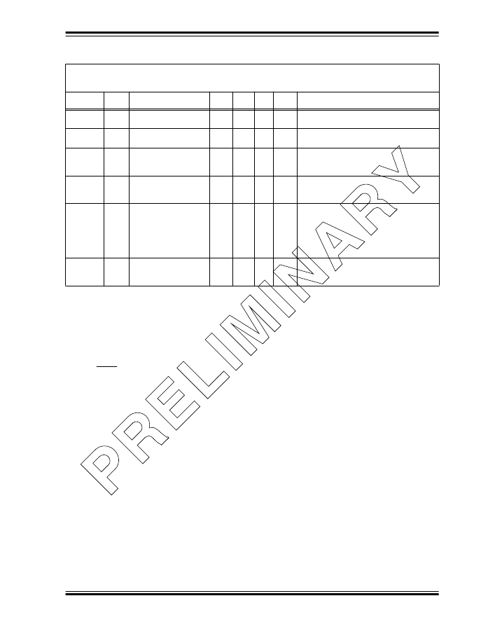
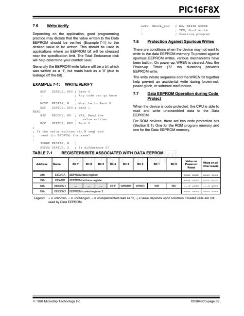
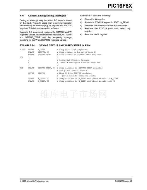
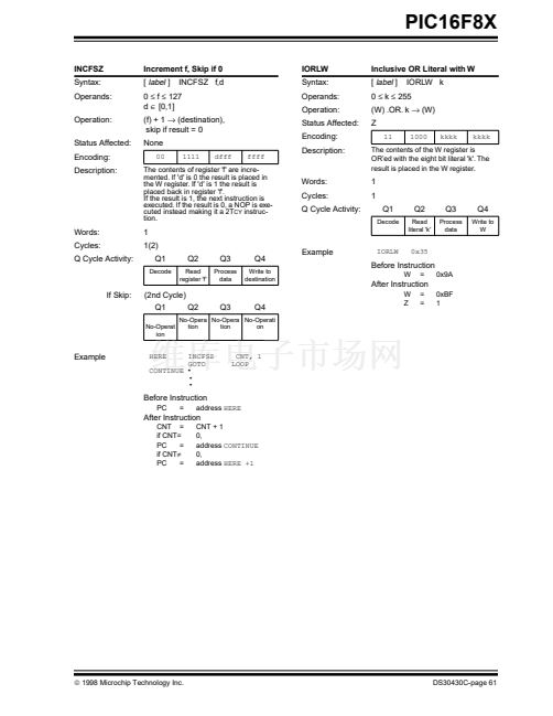
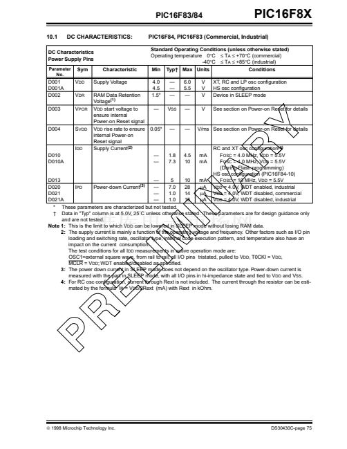
鈥?/div>
D021A
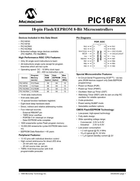
1.0
16
碌A
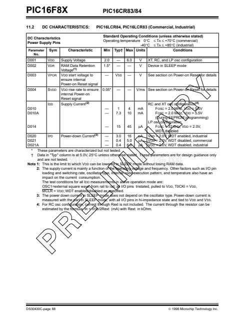
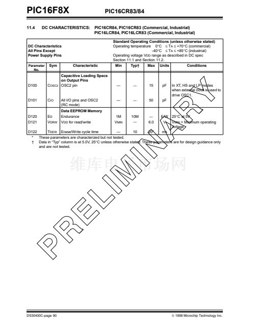
* These parameters are characterized but not tested.
鈥?Data in "Typ" column is at 5.0V, 25藲C unless otherwise stated. These parameters are for design guidance only
and are not tested.
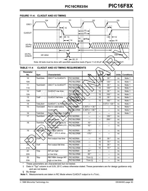
Note 1:
This is the limit to which V
DD
can be lowered in SLEEP mode without losing RAM data.
2:
The supply current is mainly a function of the operating voltage and frequency. Other factors such as I/O pin
loading and switching rate, oscillator type, internal code execution pattern, and temperature also have an
impact on the current consumption.
The test conditions for all I
DD
measurements in active operation mode are:
OSC1=external square wave, from rail to rail; all I/O pins tristated, pulled to V
DD
, T0CKI = V
DD
,
MCLR = V
DD
; WDT enabled/disabled as speci铿乪d.
3:
The power down current in SLEEP mode does not depend on the oscillator type. Power-down current is
measured with the part in SLEEP mode, with all I/O pins in hi-impedance state and tied to V
DD
and V
SS
.
4:
For RC osc con铿乬uration, current through Rext is not included. The current through the resistor can be esti-
mated by the formula I
R
= V
DD
/2Rext (mA) with Rext in kOhm.
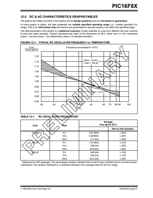
RC and XT osc con铿乬uration
(4)
F
OSC
= 4.0 MHz, V
DD
= 5.5V
F
OSC
= 4.0 MHz, V
DD
= 5.5V
(During EEPROM programming)
HS
OSC CONFIGURATION
(PIC16CR84-10)
F
OSC
= 10 MHz, V
DD
= 5.5V
V
DD
= 4.0V, WDT enabled, industrial
V
DD
= 4.0V, WDT disabled, commercial
V
DD
= 4.0V, WDT disabled, industrial
漏
1998 Microchip Technology Inc.
DS30430C-page 87


 1
1
 2
2
 3
3
 4
4
 5
5
 6
6
 7
7
 8
8
 9
9
 10
10
 11
11
 12
12
 13
13
 14
14
 15
15
 16
16
 17
17
 18
18
 19
19
 20
20
 21
21
 22
22
 23
23
 24
24
 25
25
 26
26
 27
27
 28
28
 29
29
 30
30
 31
31
 32
32
 33
33
 34
34
 35
35
 36
36
 37
37
 38
38
 39
39
 40
40
 41
41
 42
42
 43
43
 44
44
 45
45
 46
46
 47
47
 48
48
 49
49
 50
50
 51
51
 52
52
 53
53
 54
54
 55
55
 56
56
 57
57
 58
58
 59
59
 60
60
 61
61
 62
62
 63
63
 64
64
 65
65
 66
66
 67
67
 68
68
 69
69
 70
70
 71
71
 72
72
 73
73
 74
74
 75
75
 76
76
 77
77
 78
78
 79
79
 80
80
 81
81
 82
82
 83
83
 84
84
 85
85
 86
86
 87
87
 88
88
 89
89
 90
90
 91
91
 92
92
 93
93
 94
94
 95
95
 96
96
 97
97
 98
98
 99
99
 100
100
 101
101
 102
102
 103
103
 104
104
 105
105
 106
106
 107
107
 108
108
 109
109
 110
110
 111
111
 112
112
 113
113
 114
114
 115
115
 116
116
 117
117
 118
118
 119
119
 120
120
 121
121
 122
122
 123
123
 124
124
