鈥?/div>
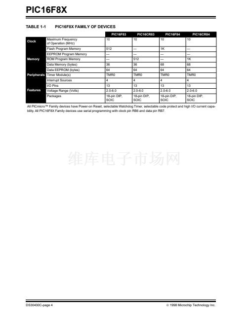
External interrupt RB0/INT pin
TMR0 over铿俹w interrupt
PORTB change interrupts (pins RB7:RB4)
Data EEPROM write complete interrupt
The RB0/INT pin interrupt, the RB port change inter-
rupt and the TMR0 over铿俹w interrupt 铿俛gs are con-
tained in the INTCON register.
When an interrupt is responded to; the GIE bit is
cleared to disable any further interrupt, the return
address is pushed onto the stack and the PC is loaded
with 0004h. For external interrupt events, such as the
RB0/INT pin or PORTB change interrupt, the interrupt
latency will be three to four instruction cycles. The exact
latency depends when the interrupt event occurs
(Figure 8-17). The latency is the same for both one and
two cycle instructions. Once in the interrupt service
routine the source(s) of the interrupt can be determined
by polling the interrupt 铿俛g bits. The interrupt 铿俛g bit(s)
must be cleared in software before re-enabling
interrupts to avoid in铿乶ite interrupt requests.
The interrupt control register (INTCON) records
individual interrupt requests in 铿俛g bits. It also contains
the individual and global interrupt enable bits.
The global interrupt enable bit, GIE (INTCON<7>)
enables (if set) all un-masked interrupts or disables (if
cleared) all interrupts. Individual interrupts can be
disabled through their corresponding enable bits in
INTCON register. Bit GIE is cleared on reset.
The 鈥渞eturn from interrupt鈥?instruction,
RETFIE,
exits
interrupt routine as well as sets the GIE bit, which
re-enable interrupts.
Note 1:
Individual interrupt 铿俛g bits are set
regardless of the status of their
corresponding mask bit or the GIE bit.
FIGURE 8-16: INTERRUPT LOGIC
T0IF
T0IE
INTF
INTE
RBIF
RBIE
EEIF
EEIE
GIE
Wake-up
(If in SLEEP mode)
Interrupt to CPU
漏
1998 Microchip Technology Inc.
DS30430C-page 47


 1
1
 2
2
 3
3
 4
4
 5
5
 6
6
 7
7
 8
8
 9
9
 10
10
 11
11
 12
12
 13
13
 14
14
 15
15
 16
16
 17
17
 18
18
 19
19
 20
20
 21
21
 22
22
 23
23
 24
24
 25
25
 26
26
 27
27
 28
28
 29
29
 30
30
 31
31
 32
32
 33
33
 34
34
 35
35
 36
36
 37
37
 38
38
 39
39
 40
40
 41
41
 42
42
 43
43
 44
44
 45
45
 46
46
 47
47
 48
48
 49
49
 50
50
 51
51
 52
52
 53
53
 54
54
 55
55
 56
56
 57
57
 58
58
 59
59
 60
60
 61
61
 62
62
 63
63
 64
64
 65
65
 66
66
 67
67
 68
68
 69
69
 70
70
 71
71
 72
72
 73
73
 74
74
 75
75
 76
76
 77
77
 78
78
 79
79
 80
80
 81
81
 82
82
 83
83
 84
84
 85
85
 86
86
 87
87
 88
88
 89
89
 90
90
 91
91
 92
92
 93
93
 94
94
 95
95
 96
96
 97
97
 98
98
 99
99
 100
100
 101
101
 102
102
 103
103
 104
104
 105
105
 106
106
 107
107
 108
108
 109
109
 110
110
 111
111
 112
112
 113
113
 114
114
 115
115
 116
116
 117
117
 118
118
 119
119
 120
120
 121
121
 122
122
 123
123
 124
124
