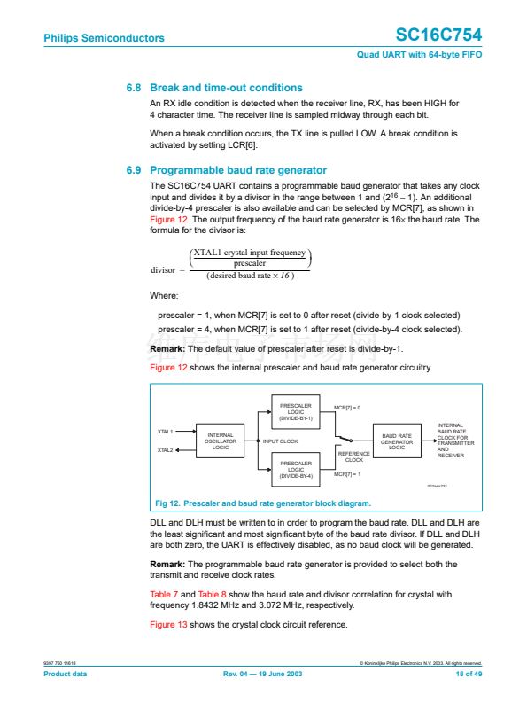
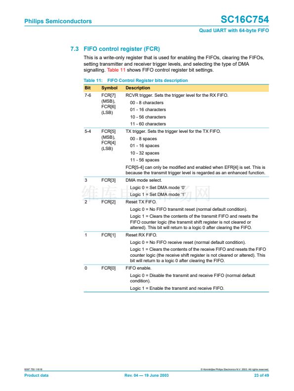
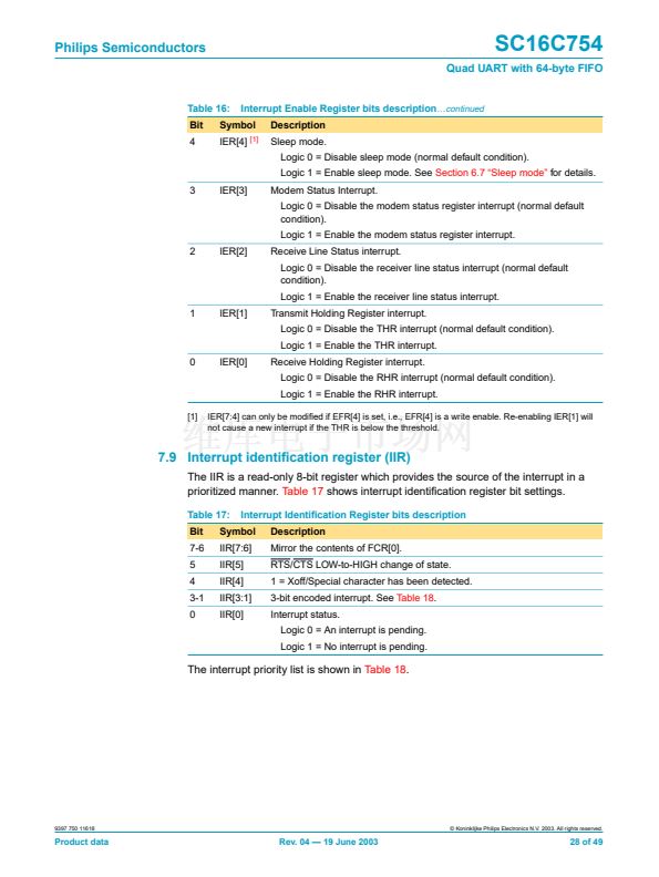
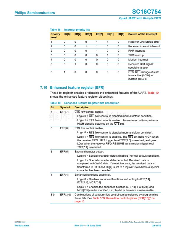
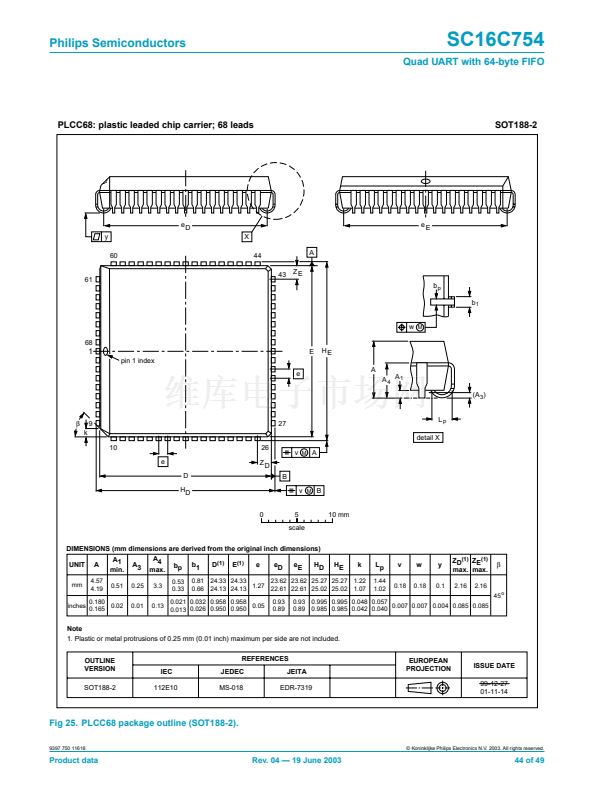
Philips Semiconductors
SC16C754
Quad UART with 64-byte FIFO
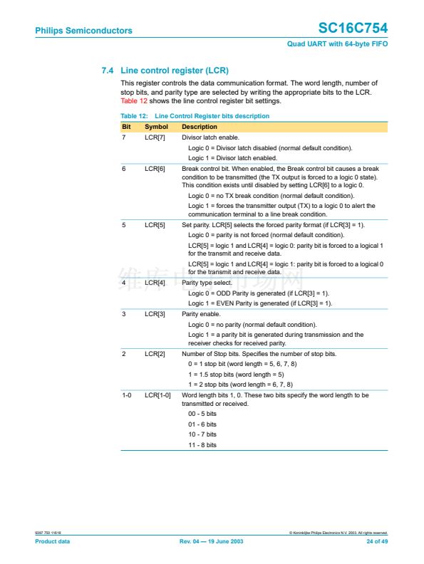
7.4 Line control register (LCR)
This register controls the data communication format. The word length, number of
stop bits, and parity type are selected by writing the appropriate bits to the LCR.
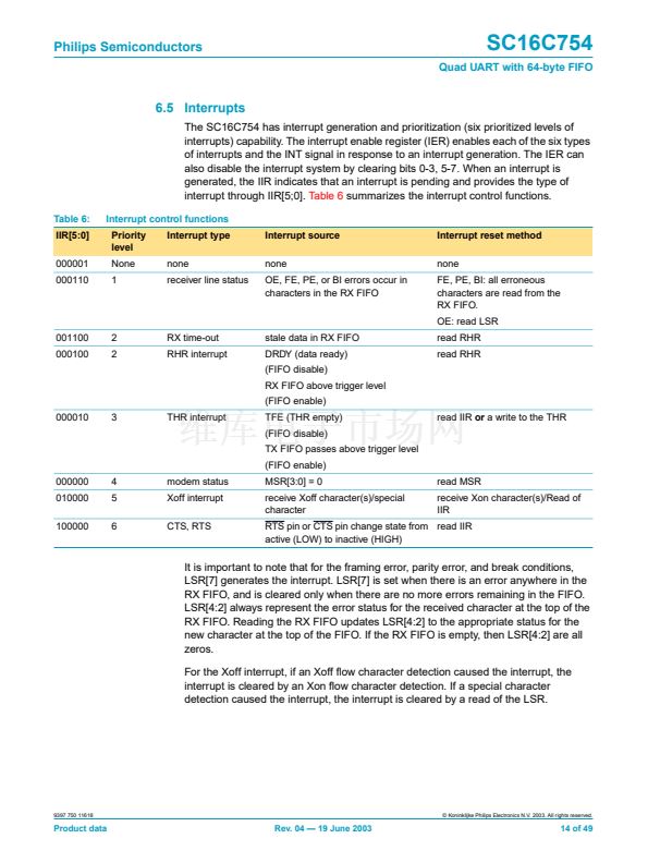
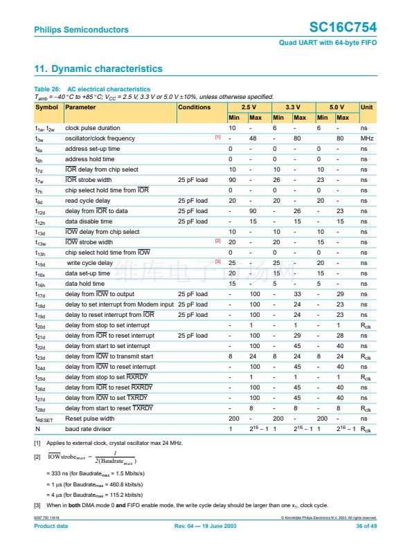
Table 12
shows the line control register bit settings.
Table 12:
Bit
7
Line Control Register bits description
Description
Divisor latch enable.
Logic 0 = Divisor latch disabled (normal default condition).
Logic 1 = Divisor latch enabled.
6
LCR[6]
Break control bit. When enabled, the Break control bit causes a break
condition to be transmitted (the TX output is forced to a logic 0 state).
This condition exists until disabled by setting LCR[6] to a logic 0.
Logic 0 = no TX break condition (normal default condition).
Logic 1 = forces the transmitter output (TX) to a logic 0 to alert the
communication terminal to a line break condition.
5
LCR[5]
Set parity. LCR[5] selects the forced parity format (if LCR[3] = 1).
Logic 0 = parity is not forced (normal default condition).
LCR[5] = logic 1 and LCR[4] = logic 0: parity bit is forced to a logical 1
for the transmit and receive data.
LCR[5] = logic 1 and LCR[4] = logic 1: parity bit is forced to a logical 0
for the transmit and receive data.
4
LCR[4]
Parity type select.
Logic 0 = ODD Parity is generated (if LCR[3] = 1).
Logic 1 = EVEN Parity is generated (if LCR[3] = 1).
3
LCR[3]
Parity enable.
Logic 0 = no parity (normal default condition).
Logic 1 = a parity bit is generated during transmission and the
receiver checks for received parity.
2
LCR[2]
Number of Stop bits. Speci铿乪s the number of stop bits.
0 = 1 stop bit (word length = 5, 6, 7, 8)
1 = 1.5 stop bits (word length = 5)
1 = 2 stop bits (word length = 6, 7, 8)
1-0
LCR[1-0]
Word length bits 1, 0. These two bits specify the word length to be
transmitted or received.
00 - 5 bits
01 - 6 bits
10 - 7 bits
11 - 8 bits
Symbol
LCR[7]
9397 750 11618
漏 Koninklijke Philips Electronics N.V. 2003. All rights reserved.
Product data
Rev. 04 鈥?19 June 2003
24 of 49


 1
1
 2
2
 3
3
 4
4
 5
5
 6
6
 7
7
 8
8
 9
9
 10
10
 11
11
 12
12
 13
13
 14
14
 15
15
 16
16
 17
17
 18
18
 19
19
 20
20
 21
21
 22
22
 23
23
 24
24
 25
25
 26
26
 27
27
 28
28
 29
29
 30
30
 31
31
 32
32
 33
33
 34
34
 35
35
 36
36
 37
37
 38
38
 39
39
 40
40
 41
41
 42
42
 43
43
 44
44
 45
45
 46
46
 47
47
 48
48
 49
49
