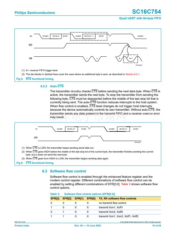
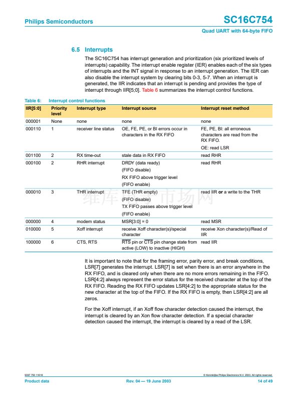
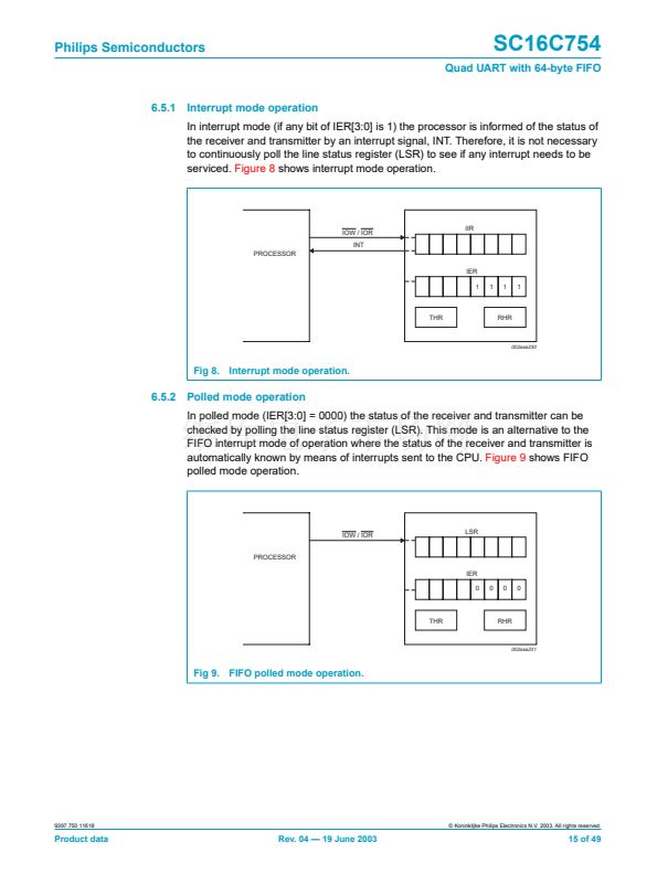
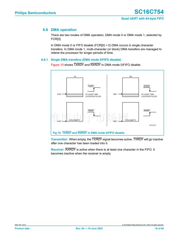
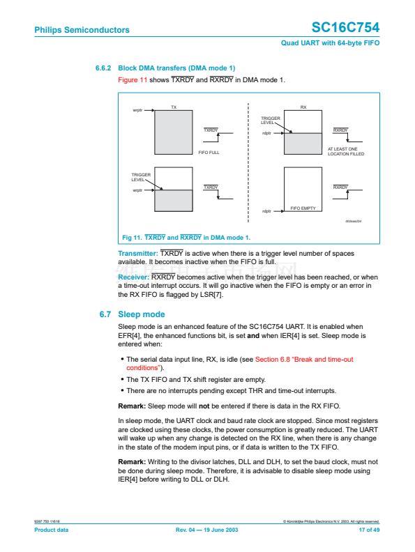
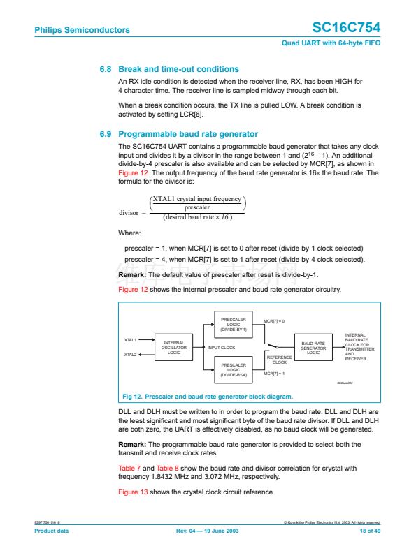
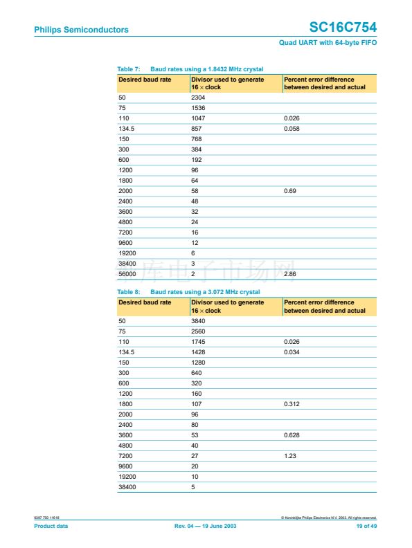
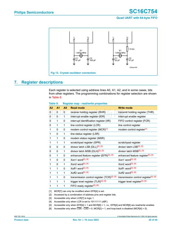
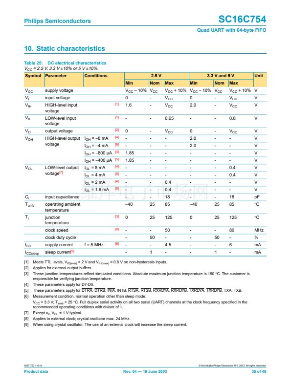
鈭?/div>
10% V
CC
Unit
V
CC
+ 10% V
V
CC
V
CC
0.8
V
CC
-
-
-
-
0.4
0.4
-
-
18
85
125
80
-
6
-
V
V
V
V
V
V
V
V
V
V
V
V
pF
掳C
掳C
MHz
%
mA
mA
[1]
[2]
[4]
[5]
[4]
[5]
[4]
[5]
[4]
[5]
[8]
supply current
sleep current
[9]
-
-
Meets TTL levels, V
IO(min)
= 2 V and V
IH(max)
= 0.8 V on non-hysteresis inputs.
Applies for external output buffers.
These junction temperatures re铿俥ct simulated conditions. Absolute maximum junction temperature is 150
掳C.
The customer is
responsible for verifying junction temperature.
These parameters apply for D7-D0.
These parameters apply for DTRA, DTRB, INIA, INTB, RTSA, RTSB, RXRDYA, RXRDYB, TXRDYA, TXRDYB, TXA, TXB.
Measurement condition, normal operation other than sleep mode:
V
CC
= 3.3 V; T
amb
= 25
掳C.
Full duplex serial activity on all two serial (UART) channels at the clock frequency speci铿乪d in the
recommended operating conditions with divisor of 1.
Except x
2
, V
OL
= 1 V typical.
Applies to external clock; crystal oscillator max. 24 MHz.
When using crystal oscillator. The use of an external clock will increase the sleep current.
[7]
[8]
[9]
9397 750 11618
漏 Koninklijke Philips Electronics N.V. 2003. All rights reserved.
Product data
Rev. 04 鈥?19 June 2003
35 of 49


 1
1
 2
2
 3
3
 4
4
 5
5
 6
6
 7
7
 8
8
 9
9
 10
10
 11
11
 12
12
 13
13
 14
14
 15
15
 16
16
 17
17
 18
18
 19
19
 20
20
 21
21
 22
22
 23
23
 24
24
 25
25
 26
26
 27
27
 28
28
 29
29
 30
30
 31
31
 32
32
 33
33
 34
34
 35
35
 36
36
 37
37
 38
38
 39
39
 40
40
 41
41
 42
42
 43
43
 44
44
 45
45
 46
46
 47
47
 48
48
 49
49
