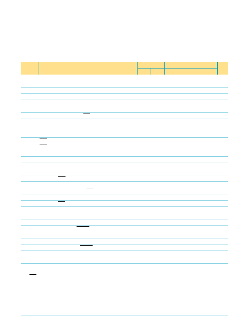
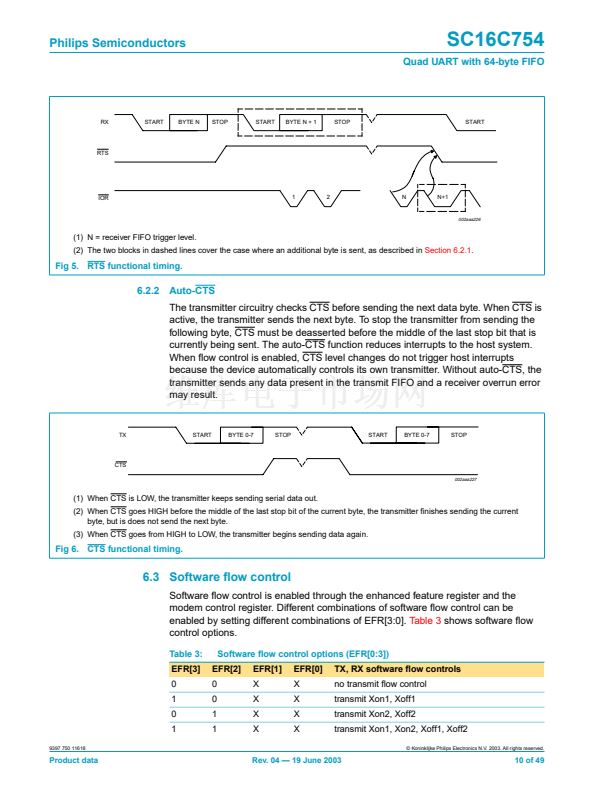
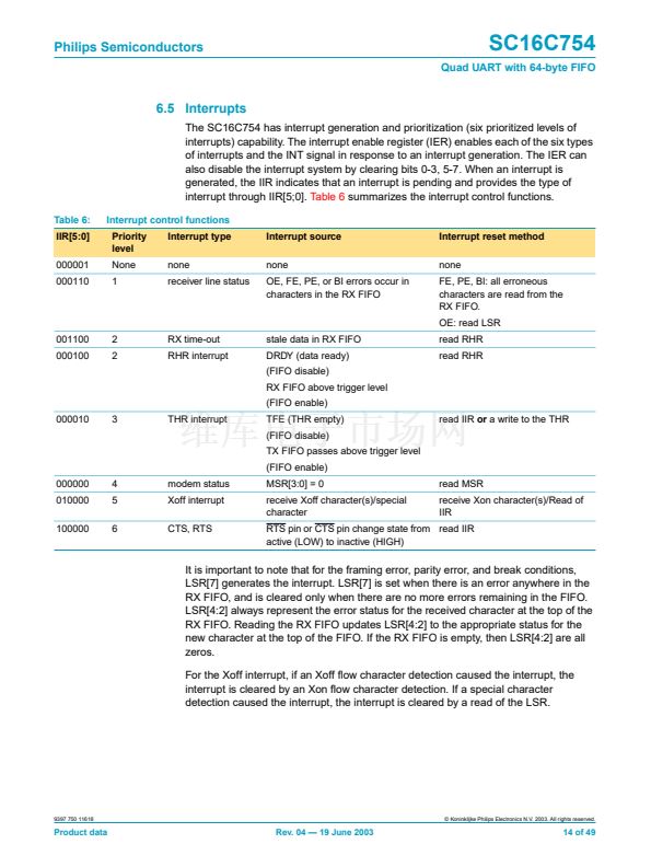
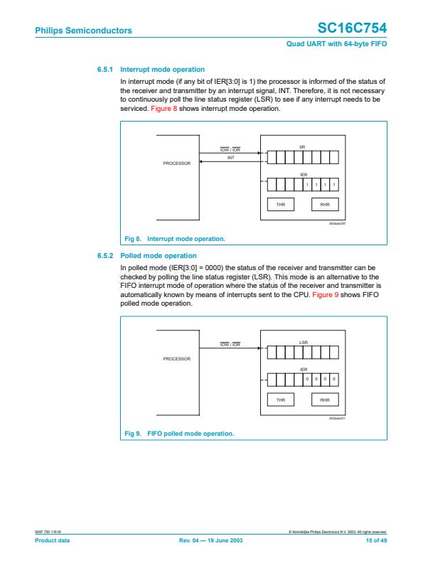
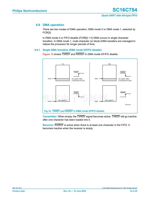
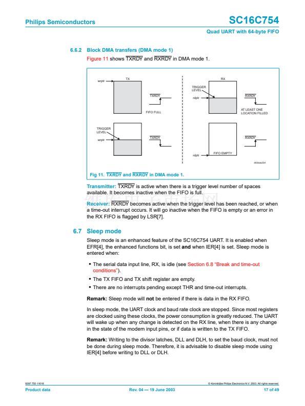
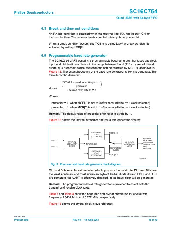
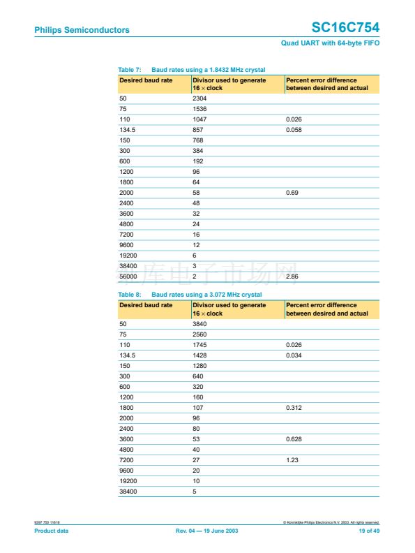
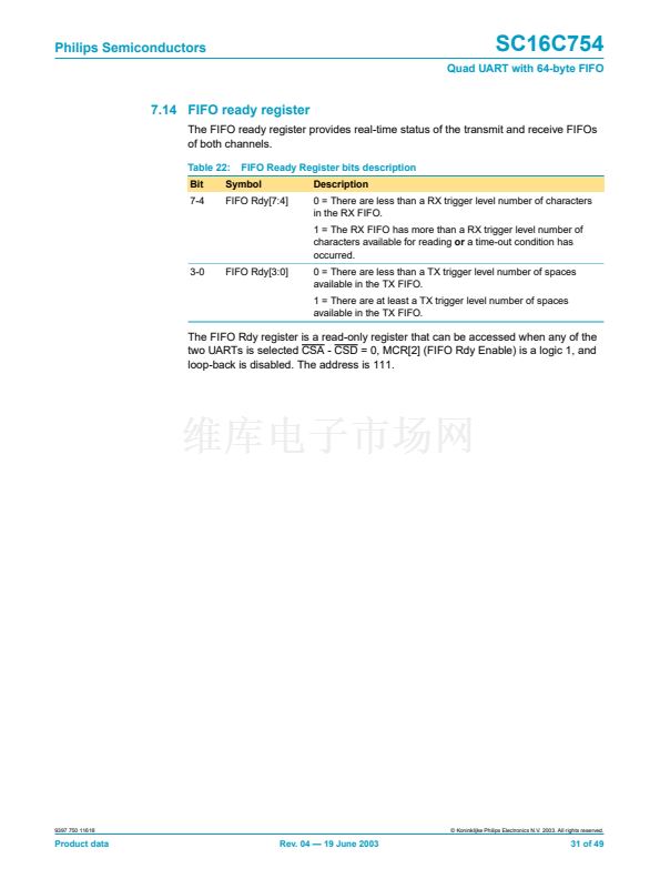
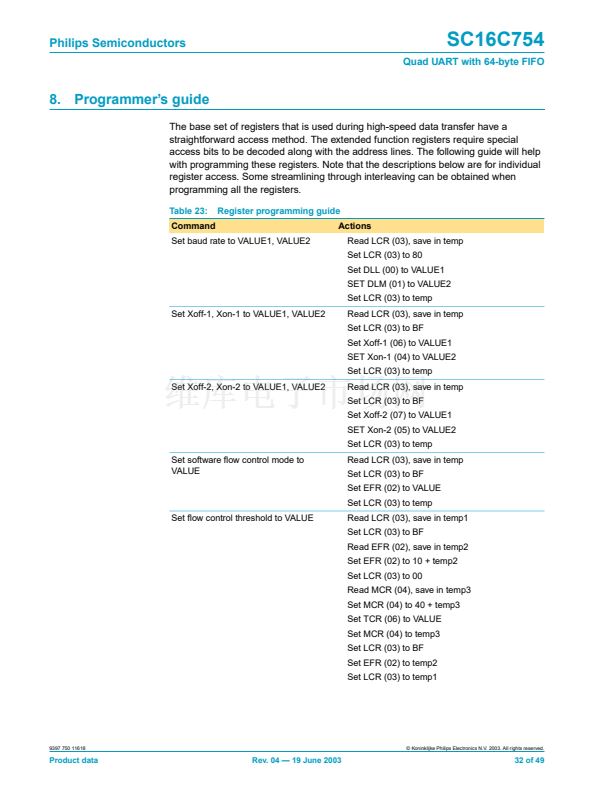
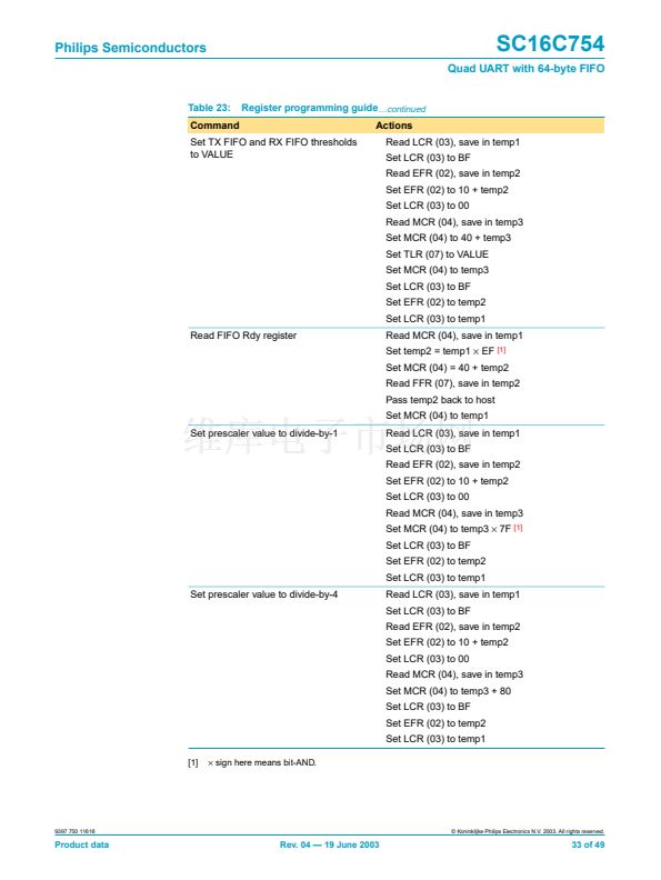
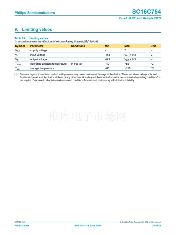
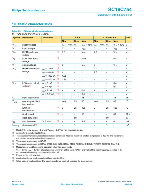
11. Dynamic characteristics
鈭?/div>
40
掳
C to +85
掳
C; V
CC
= 2.5 V, 3.3 V or 5.0 V
卤
10%, unless otherwise speci铿乪d.
Symbol
t
1w
, t
2w
t
3w
t
6s
t
6h
t
7d
t
7w
t
7h
t
9d
t
12d
t
12h
t
13d
t
13w
t
13h
t
15d
t
16s
t
16h
t
17d
t
18d
t
19d
t
20d
t
21d
t
22d
t
23d
t
24d
t
25d
t
26d
t
27d
t
28d
t
RESET
N
[1]
[2]
Parameter
clock pulse duration
oscillator/clock frequency
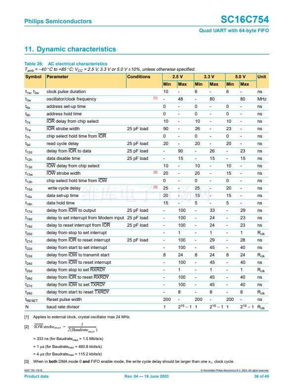
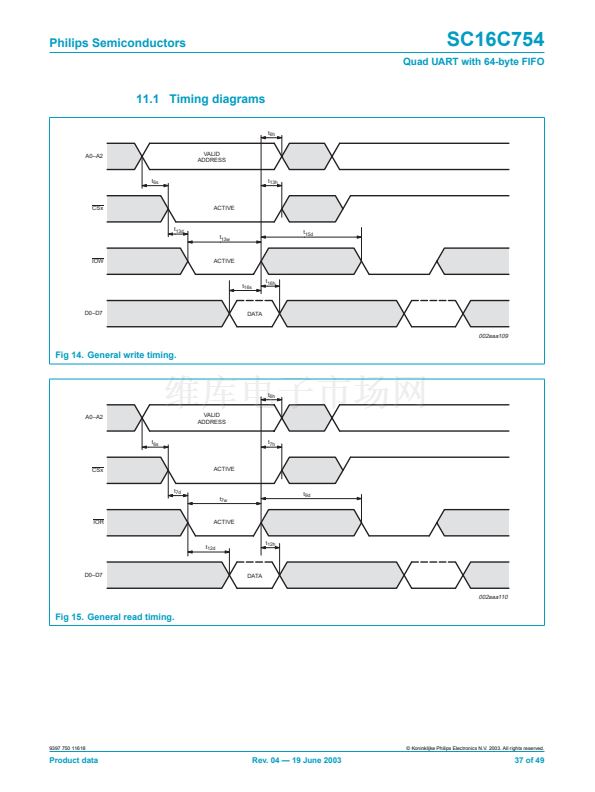
address set-up time
address hold time
IOR delay from chip select
IOR strobe width
chip select hold time from IOR
read cycle delay
delay from IOR to data
data disable time
IOW delay from chip select
IOW strobe width
chip select hold time from IOW
write cycle delay
data set-up time
data hold time
delay from IOW to output
delay to reset interrupt from IOR
delay from stop to set interrupt
delay from IOR to reset interrupt
delay from start to set interrupt
delay from IOW to transmit start
delay from IOW to reset interrupt
delay from stop to set RXRDY
delay from IOR to reset RXRDY
delay from IOW to set TXRDY
delay from start to reset TXRDY
Reset pulse width
baud rate divisor
Conditions
Min
10
[1]
2.5 V
Max
-
48
-
-
-
-
-
-
90
15
-
-
-
-
-
-
100
100
100
1
100
100
24
100
1
100
100
8
-
Min
6
-
0
0
10
26
0
20
-
-
10
20
0
25
15
5
-
-
-
-
-
-
8
-
-
-
-
-
200
3.3 V
Max
-
80
-
-
-
-
-
-
26
15
-
-
-
-
-
-
33
24
24
1
29
45
24
45
1
45
45
8
-
0
0
10
23
0
20
-
-
10
15
0
20
15
5
-
-
-
-
-
-
8
-
-
-
-
-
200
Min
6
5.0 V
Max
-
80
-
-
-
-
-
-
23
15
-
-
-
-
-
-
29
23
23
1
28
40
24
40
1
40
40
8
-
Unit
ns
MHz
ns
ns
ns
ns
ns
ns
ns
ns
ns
ns
ns
ns
ns
ns
ns
ns
ns
R
clk
ns
ns
R
clk
ns
R
clk
ns
ns
R
clk
ns
-
0
0
10
25 pF load
25 pF load
25 pF load
25 pF load
[2]
90
0
20
-
-
10
20
0
[3]
25
20
15
25 pF load
25 pF load
25 pF load
-
-
-
-
-
-
8
-
-
-
-
-
200
1
delay to set interrupt from Modem input 25 pF load
2
16
鈭?/div>
1 1
2
16
鈭?/div>
1 1
2
16
鈭?/div>
1 R
clk
Applies to external clock, crystal oscillator max 24 MHz.
1
IOWstrobe
max
=
-------------------------------------
-
2
(
Baudrate
max
)
= 333 ns (for Baudrate
max
= 1.5 Mbits/s)
= 1
碌s
(for Baudrate
max
= 460.8 kbits/s)
= 4
碌s
(for Baudrate
max
= 115.2 kbits/s)
[3]
When in
both
DMA mode 0
and
FIFO enable mode, the write cycle delay should be larger than one x
1
, clock cycle.
漏 Koninklijke Philips Electronics N.V. 2003. All rights reserved.
9397 750 11618
Product data
Rev. 04 鈥?19 June 2003
36 of 49


 1
1
 2
2
 3
3
 4
4
 5
5
 6
6
 7
7
 8
8
 9
9
 10
10
 11
11
 12
12
 13
13
 14
14
 15
15
 16
16
 17
17
 18
18
 19
19
 20
20
 21
21
 22
22
 23
23
 24
24
 25
25
 26
26
 27
27
 28
28
 29
29
 30
30
 31
31
 32
32
 33
33
 34
34
 35
35
 36
36
 37
37
 38
38
 39
39
 40
40
 41
41
 42
42
 43
43
 44
44
 45
45
 46
46
 47
47
 48
48
 49
49
