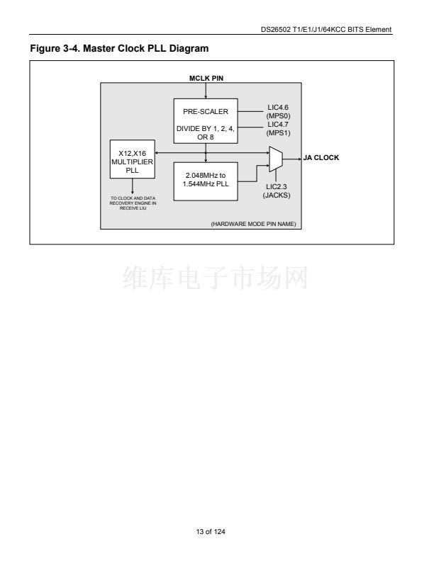
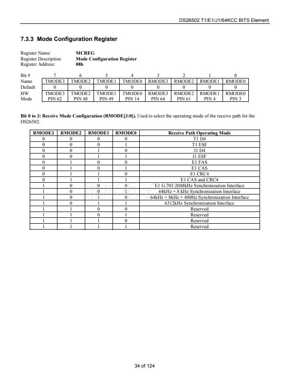
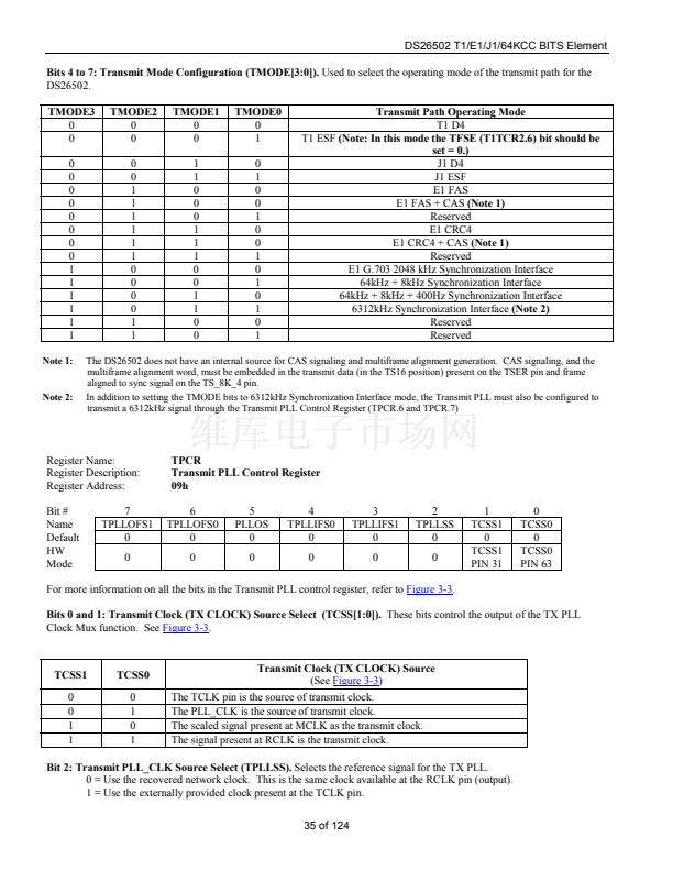
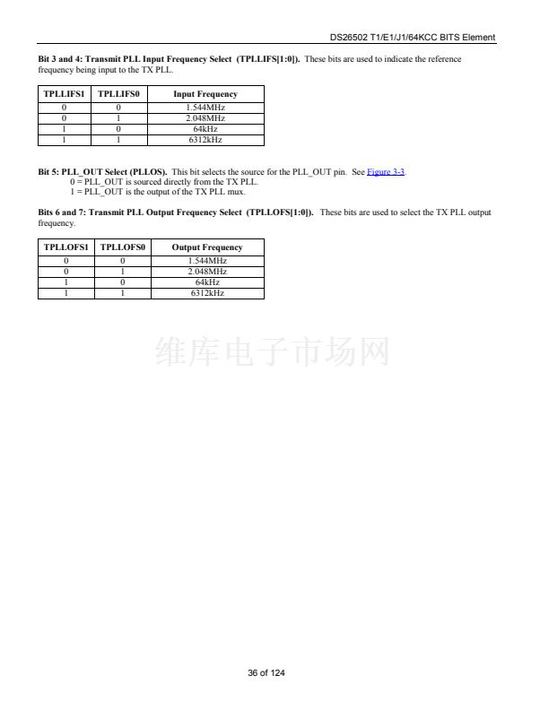
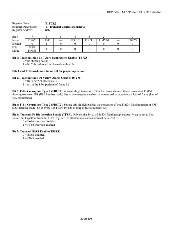
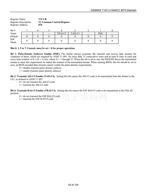
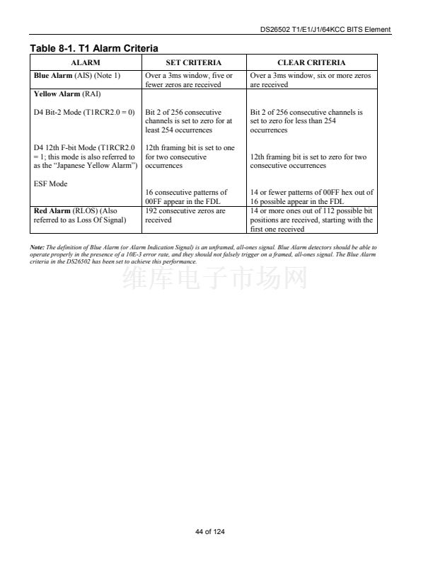
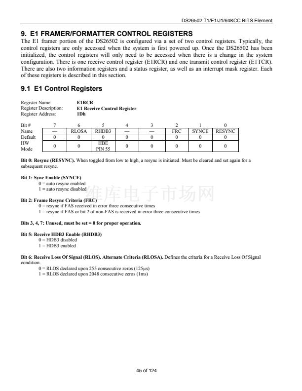
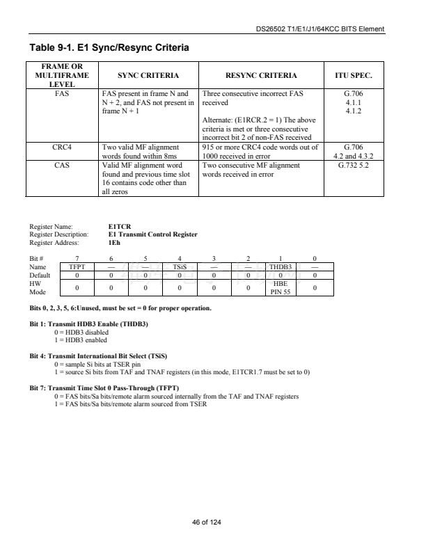
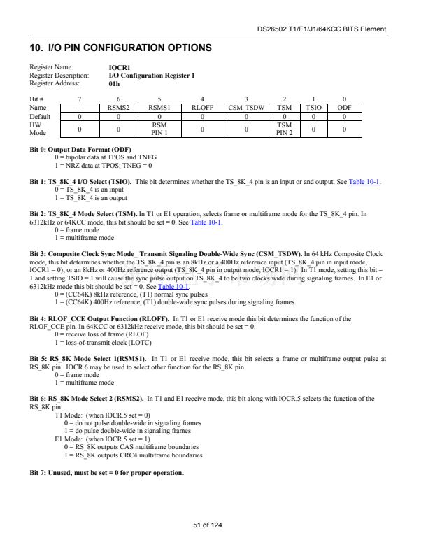
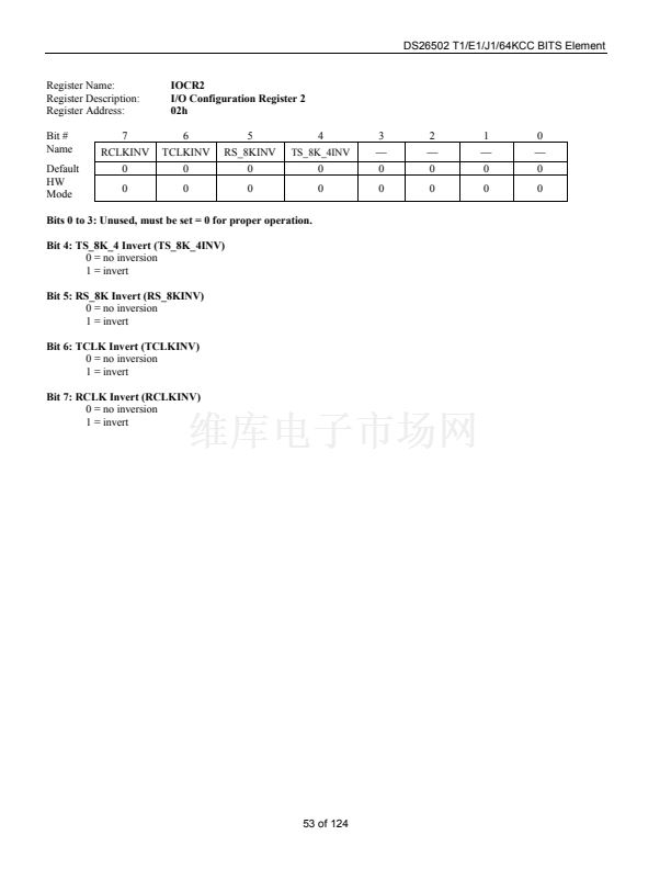
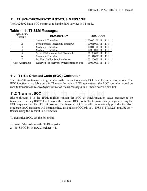
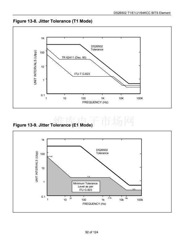
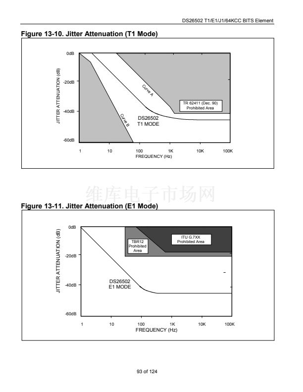
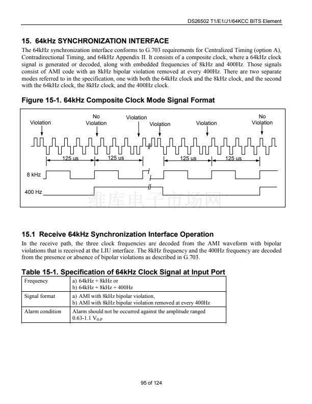
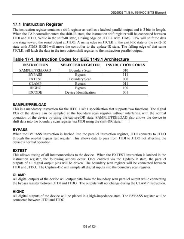
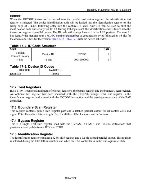
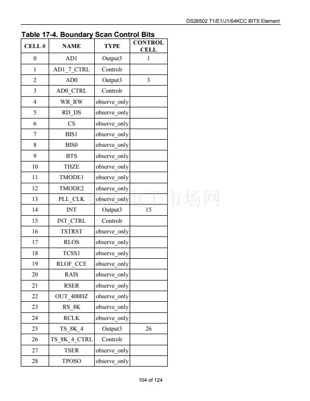
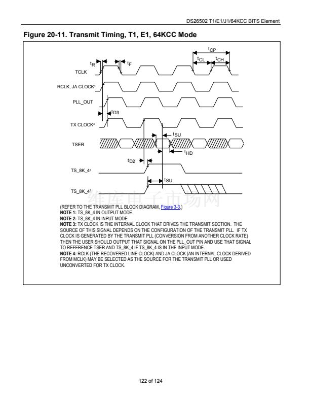
DS26502 T1/E1/J1/64KCC BITS Element
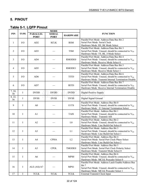
7. PROCESSOR INTERFACE
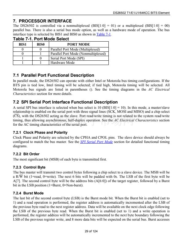
The DS26502 is controlled via a nonmultiplexed (BIS[1:0] = 01) or a multiplexed (BIS[1:0] = 00)
parallel bus. There is also a serial bus mode option, as well as a hardware mode of operation. The bus
interface type is selected by BIS1 and BIS0 as shown in
Table 7-1.
Table 7-1. Port Mode Select
BIS1
0
0
1
1
BIS0
0
1
0
1
PORT MODE
Parallel Port Mode (Multiplexed)
Parallel Port Mode (Nonmultiplexed)
Serial Port Mode (SPI)
Hardware Mode
7.1 Parallel Port Functional Description
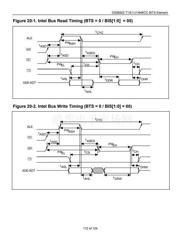
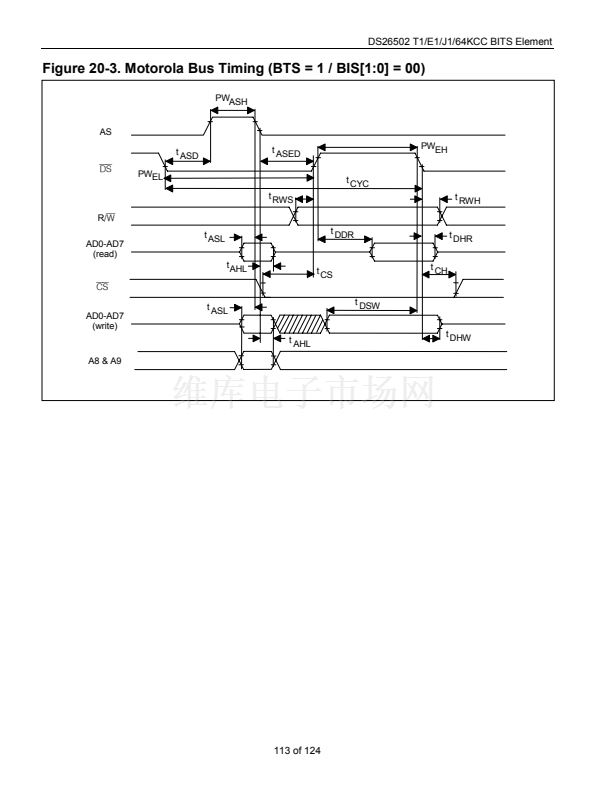
In parallel mode, the DS26502 can operate with either Intel or Motorola bus timing configurations. If the
BTS pin is tied low, Intel timing will be selected; if tied high, Motorola timing will be selected. All
Motorola bus signals are listed in parentheses (). See the timing diagrams in the
AC Electrical
Characteristics
section for more details.
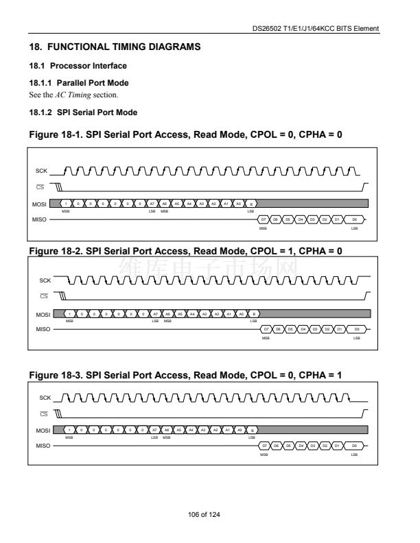
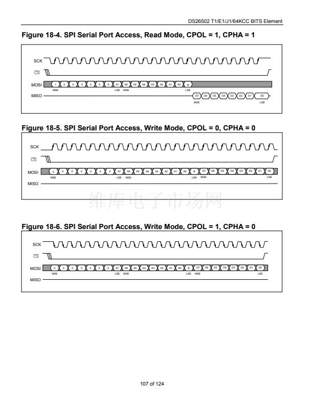
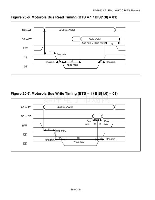
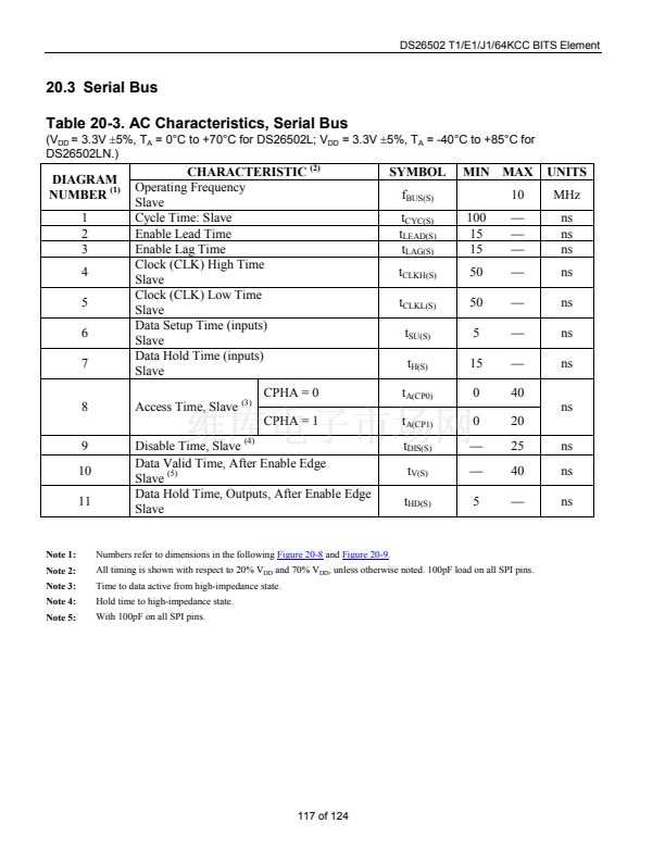
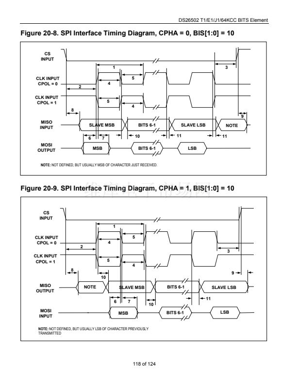
7.2 SPI Serial Port Interface Functional Description
A serial SPI bus interface is selected when bus select is 10 (BIS[1:0] = 10). In this mode, a master/slave
relationship is enabled on the serial port with three signal lines (SCK, MOSI and MISO) and a chip select
(CS), with the DS26502 acting as the slave. Port read/write timing is not related to the system read/write
timing, thus allowing asynchronous, half-duplex operation. See the
AC Electrical Characteristics
section
for the AC timing characteristics of the serial port.
7.2.1 Clock Phase and Polarity
Clock Phase and Polarity are selected by the CPHA and CPOL pins. The slave device should always be
configured to match the bus master. See the
SPI Serial Port Mode
section for detailed functional timing
diagrams.
7.2.2 Bit Order
The most significant bit (MSB) of each byte is transmitted first.
7.2.3 Control Byte
The bus master will transmit two control bytes following a chip select to a slave device. The MSB will be
a R/W bit (1=read, 0=write). The next 6 bits will be padded with 0s. The LSB of the first byte will be
A[7]. The second control byte will be the address bits (A[6:0]) of the target register, followed by a Burst
bit in the LSB position (1=Burst, 0=Non-burst).
7.2.4 Burst Mode
The last bit of the second control byte (LSB) is the Burst mode bit. When the Burst bit is enabled (set to
1) and a read operation is performed, the register address is automatically incremented after the LSB of
the previous byte read to the next register address. Data will be available on the next clock edge following
the LSB of the previous byte read. When the Burst bit is enabled (set to 1) and a write operation is
performed, the register address will be automatically incremented to the next byte boundary following the
LSB of the previous register write, and 8 more data bits will be expected on the serial bus. Burst accesses
29 of 124


 1
1
 2
2
 3
3
 4
4
 5
5
 6
6
 7
7
 8
8
 9
9
 10
10
 11
11
 12
12
 13
13
 14
14
 15
15
 16
16
 17
17
 18
18
 19
19
 20
20
 21
21
 22
22
 23
23
 24
24
 25
25
 26
26
 27
27
 28
28
 29
29
 30
30
 31
31
 32
32
 33
33
 34
34
 35
35
 36
36
 37
37
 38
38
 39
39
 40
40
 41
41
 42
42
 43
43
 44
44
 45
45
 46
46
 47
47
 48
48
 49
49
 50
50
 51
51
 52
52
 53
53
 54
54
 55
55
 56
56
 57
57
 58
58
 59
59
 60
60
 61
61
 62
62
 63
63
 64
64
 65
65
 66
66
 67
67
 68
68
 69
69
 70
70
 71
71
 72
72
 73
73
 74
74
 75
75
 76
76
 77
77
 78
78
 79
79
 80
80
 81
81
 82
82
 83
83
 84
84
 85
85
 86
86
 87
87
 88
88
 89
89
 90
90
 91
91
 92
92
 93
93
 94
94
 95
95
 96
96
 97
97
 98
98
 99
99
 100
100
 101
101
 102
102
 103
103
 104
104
 105
105
 106
106
 107
107
 108
108
 109
109
 110
110
 111
111
 112
112
 113
113
 114
114
 115
115
 116
116
 117
117
 118
118
 119
119
 120
120
 121
121
 122
122
 123
123
 124
124
