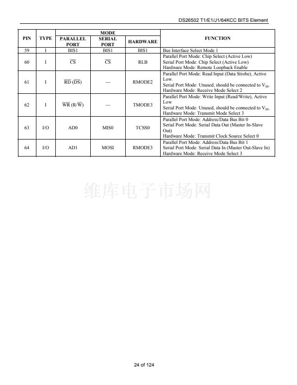
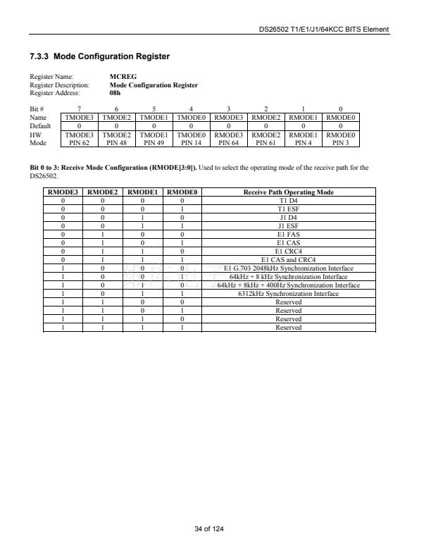
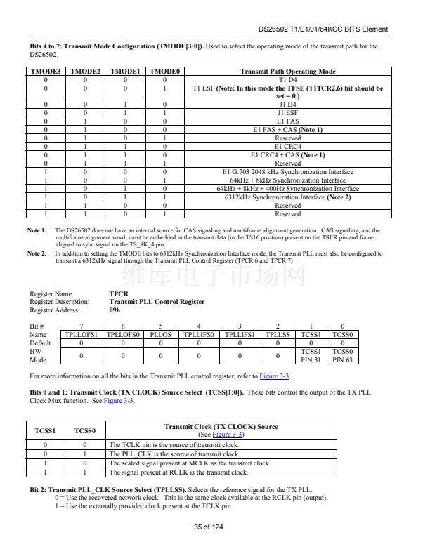
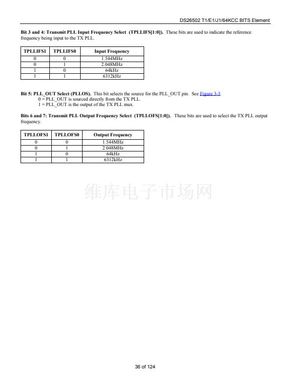
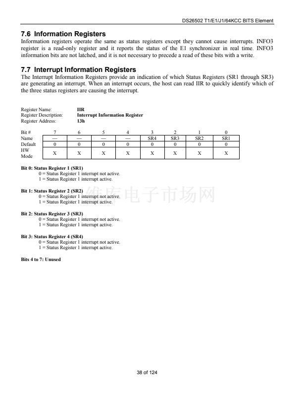
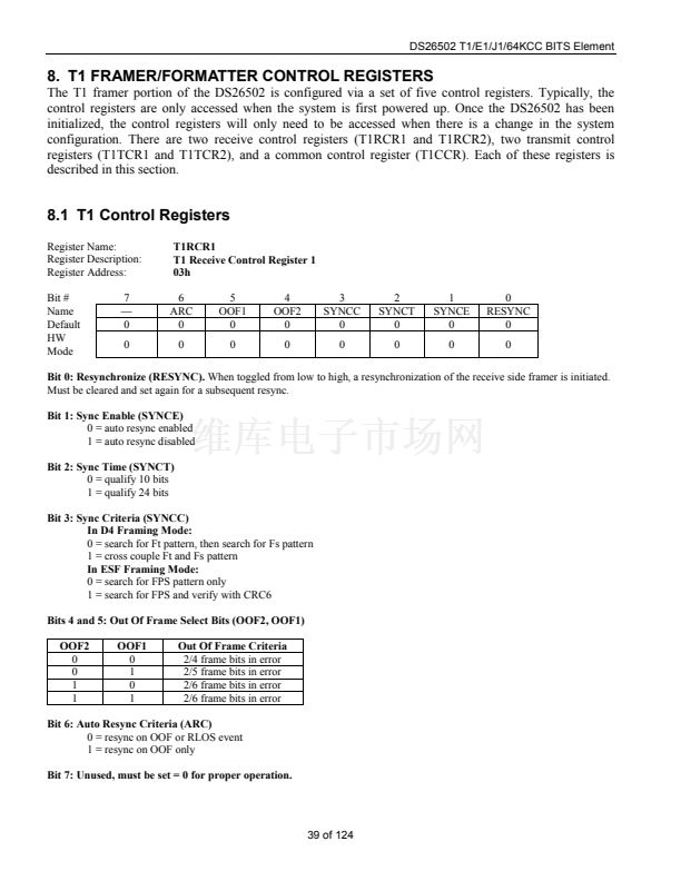
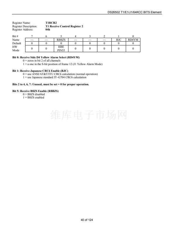
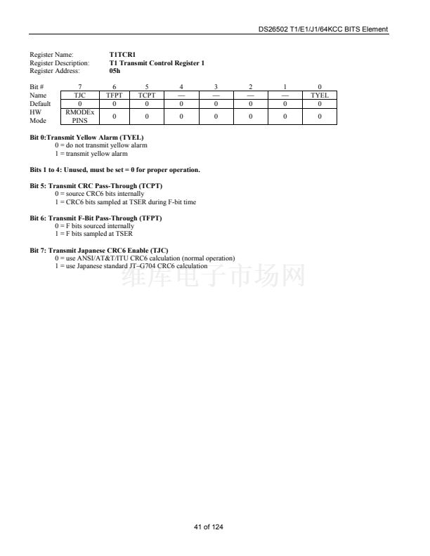
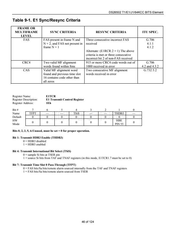
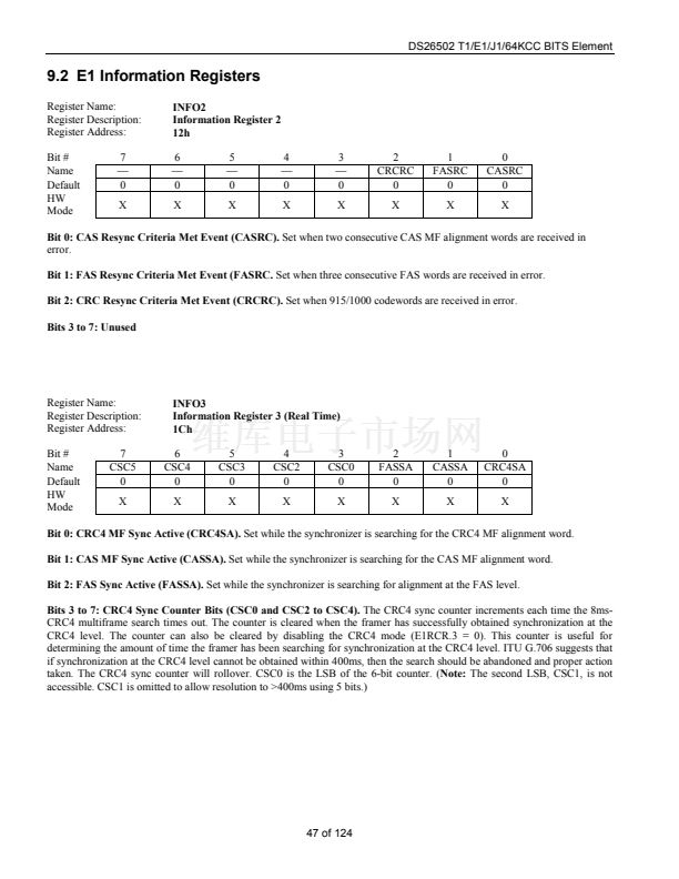
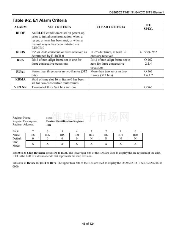
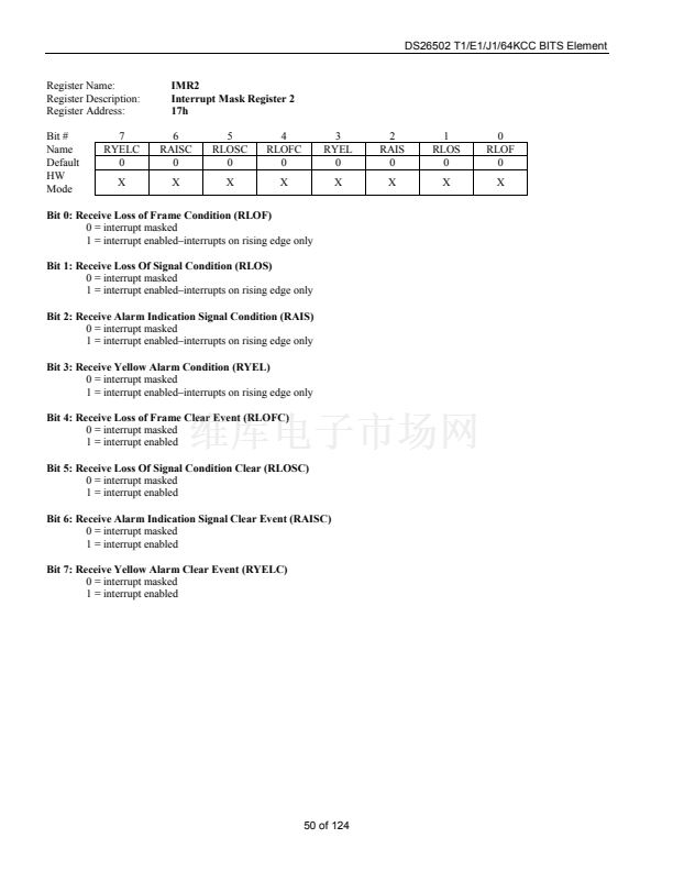
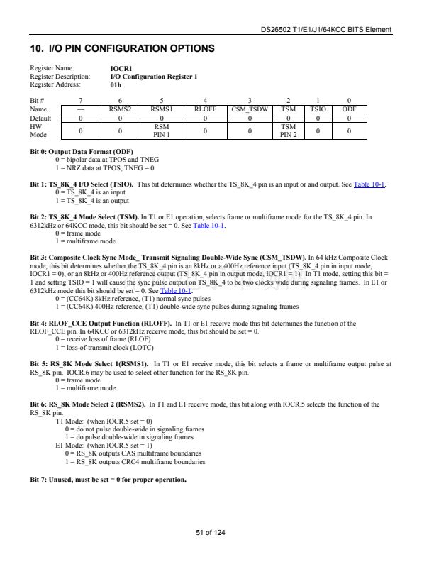
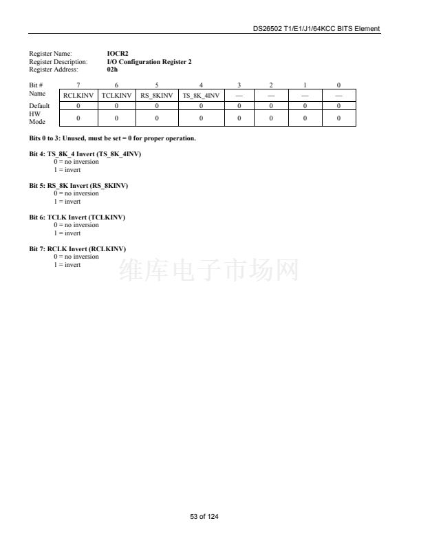
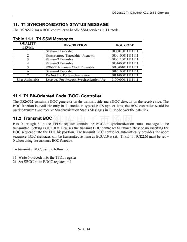
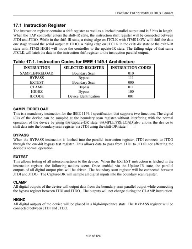
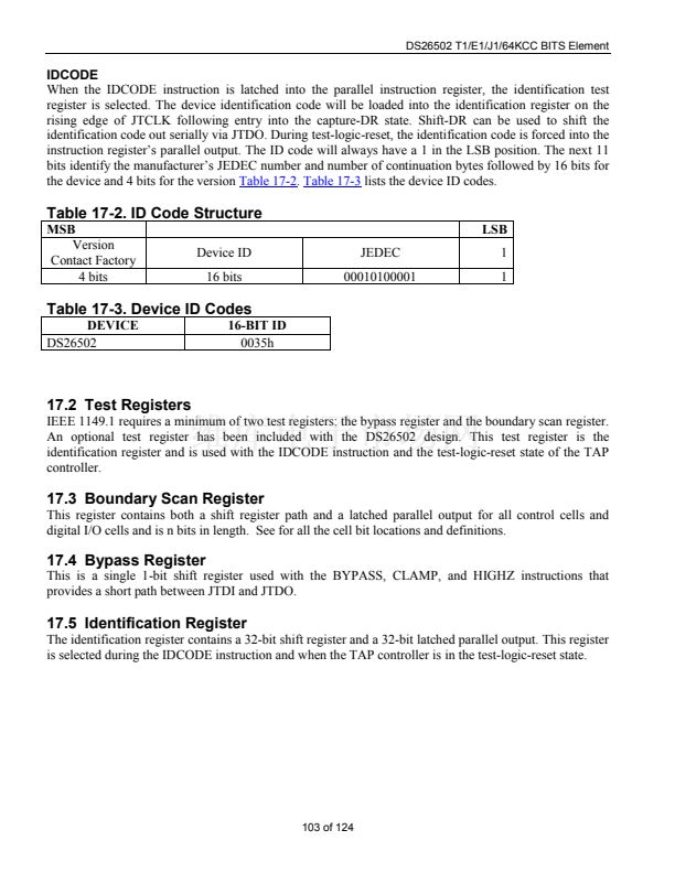
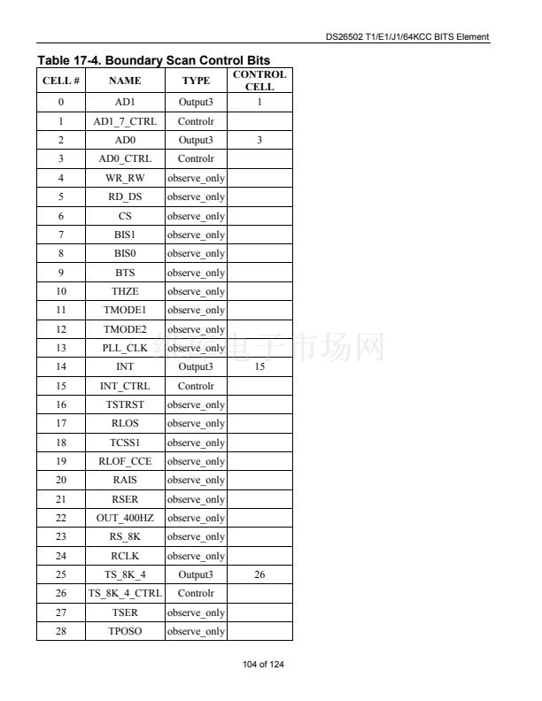
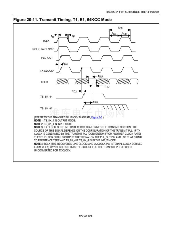
DS26502 T1/E1/J1/64KCC BITS Element
4.4 Controller Interface
NAME
TYPE
FUNCTION
Interrupt/JA Clock Source Select 1
INT:
Flags host controller during events, alarms, and conditions defined in
the status registers. Active-low open-drain output.
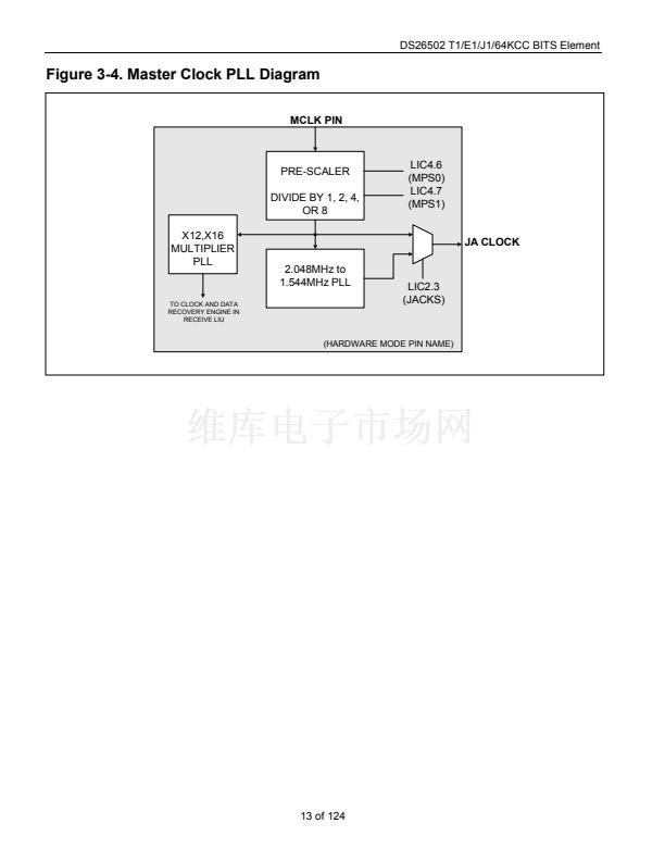
JACKS: Hardware Mode: JA Clock Select. Set this pin high for T1 mode
operation when either a 2.048MHz, 4.096MHz, 8.192MHz or 16.382MHz
signal is applied at MCLK.
Transmit Mode Select 1.
In Hardware Mode (BIS[1:0] = 11), this bit is used
to configure the transmit operating mode.
Transmit Mode Select 2.
In Hardware Mode (BIS[1:0] = 11), this bit is used
to configure the transmit operating mode.
Tri-State Control and Device Reset.
A dual-function pin. A zero-to-one
transition issues a hardware reset to the DS26502 register set. Configuration
register contents are set to the default state. Leaving TSTRST high tri-states
all output and I/O pins (including the parallel control port). Set low for
normal operation. Useful for in-board level testing.
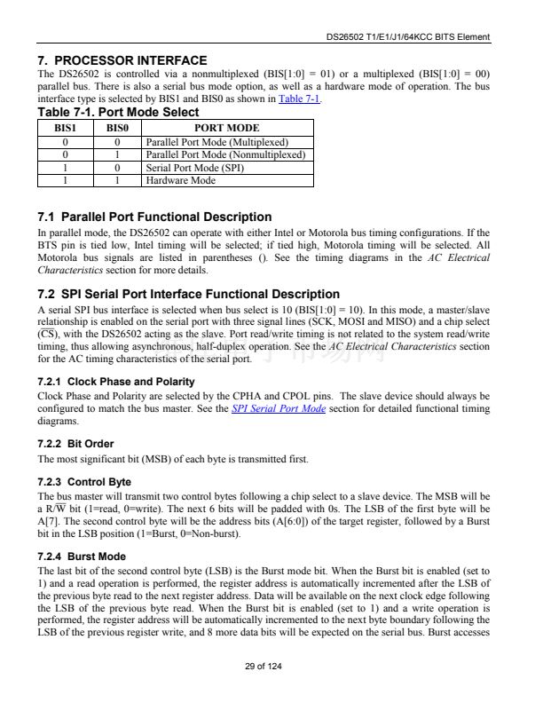
Bus Interface Mode Select 1, 0.
These bits select the controller interface
mode of operation.
BIS[1:0] : 00 = Parallel Port Mode (Multiplexed)
01 = Parallel Port Mode (Nonmultiplexed)
10 = Serial Port Mode
11 = Hardware Mode
Data Bus D[7] or Address/Data Bus AD[7]/Transmit Termination Select
A[7]: In nonmultiplexed bus operation (BIS[1:0] = 01), it serves as the data
bus D[7].
AD[7]: In multiplexed bus operation (BIS[1:0] = 00), it serves as the
multiplexed address/data bus AD[7].
RITD: In Hardware Mode (BIS[1:0] = 11), it disables the internal receive
termination.
Data Bus D[6] or Address/Data Bus AD[6]/Transmit Termination Select
A[6]: In nonmultiplexed bus operation (BIS[1:0] = 01), it serves as the data
bus D[6].
AD[6]: In multiplexed bus operation (BIS[1:0] = 00), it serves as the
multiplexed address/data bus AD[6].
TITD: In Hardware Mode (BIS[1:0] = 11), it disables the internal transmit
termination.
Data Bus D[5] or Address/Data Bus AD[5]/Receive Framing Mode Select
Bit 1
A[5]: In nonmultiplexed bus operation (BIS[1:0] = 01), it serves as the data
bus D[5].
AD[5]: In multiplexed bus operation (BIS[1:0] = 00), it serves as the
multiplexed address/data bus AD[5].
RMODE1: In Hardware Mode (BIS[1:0] = 11), it selects the receive side
operating mode.
16 of 124
INT/
JACKS
I/O
TMODE1
TMODE2
I
I
TSTRST
I
BIS[1:0]
I
AD[7]/
RITD
I/O
AD[6]/
TITD
I/O
AD[5]/
RMODE1
I/O


 1
1
 2
2
 3
3
 4
4
 5
5
 6
6
 7
7
 8
8
 9
9
 10
10
 11
11
 12
12
 13
13
 14
14
 15
15
 16
16
 17
17
 18
18
 19
19
 20
20
 21
21
 22
22
 23
23
 24
24
 25
25
 26
26
 27
27
 28
28
 29
29
 30
30
 31
31
 32
32
 33
33
 34
34
 35
35
 36
36
 37
37
 38
38
 39
39
 40
40
 41
41
 42
42
 43
43
 44
44
 45
45
 46
46
 47
47
 48
48
 49
49
 50
50
 51
51
 52
52
 53
53
 54
54
 55
55
 56
56
 57
57
 58
58
 59
59
 60
60
 61
61
 62
62
 63
63
 64
64
 65
65
 66
66
 67
67
 68
68
 69
69
 70
70
 71
71
 72
72
 73
73
 74
74
 75
75
 76
76
 77
77
 78
78
 79
79
 80
80
 81
81
 82
82
 83
83
 84
84
 85
85
 86
86
 87
87
 88
88
 89
89
 90
90
 91
91
 92
92
 93
93
 94
94
 95
95
 96
96
 97
97
 98
98
 99
99
 100
100
 101
101
 102
102
 103
103
 104
104
 105
105
 106
106
 107
107
 108
108
 109
109
 110
110
 111
111
 112
112
 113
113
 114
114
 115
115
 116
116
 117
117
 118
118
 119
119
 120
120
 121
121
 122
122
 123
123
 124
124
