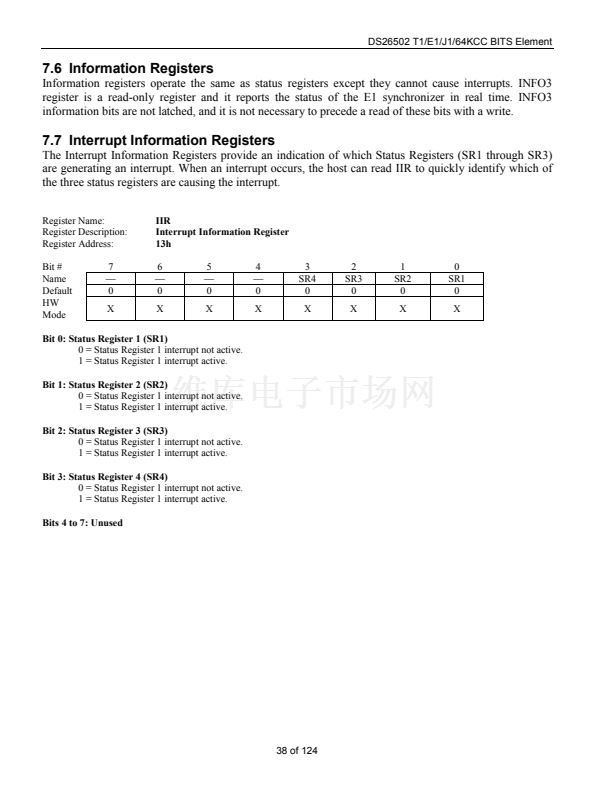
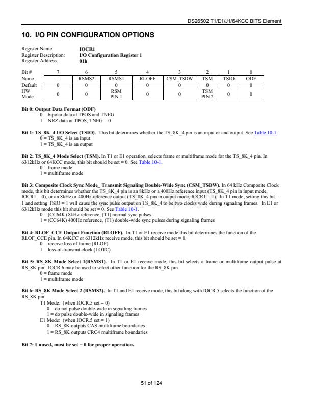
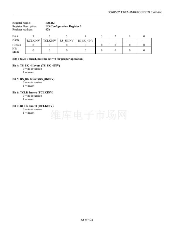
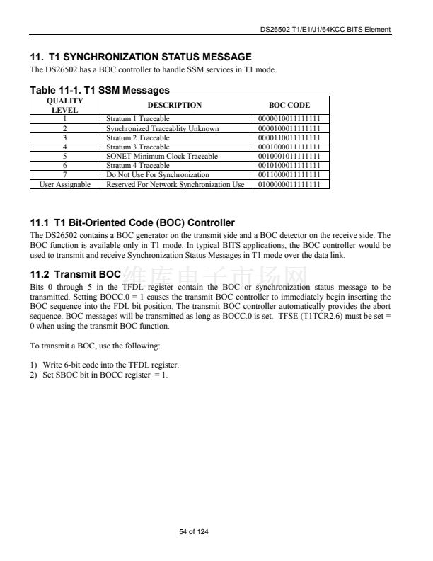
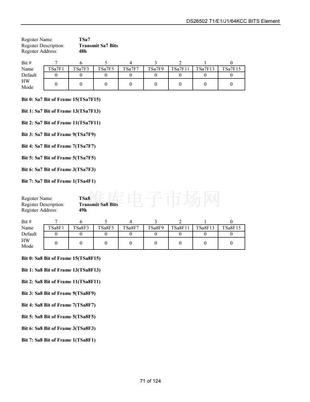
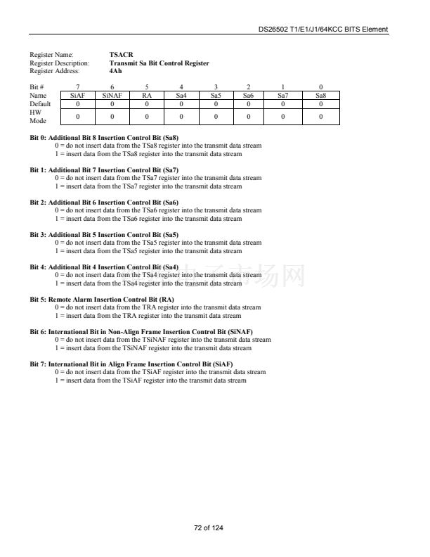
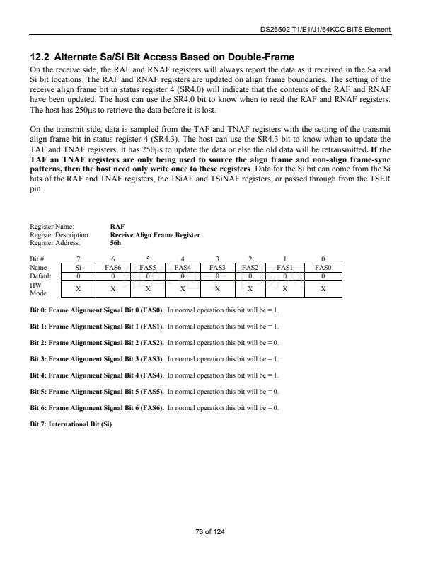
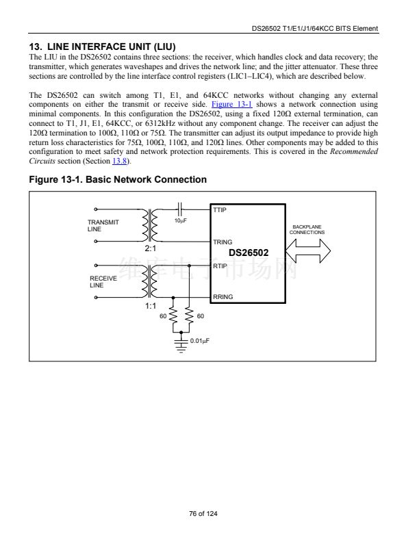
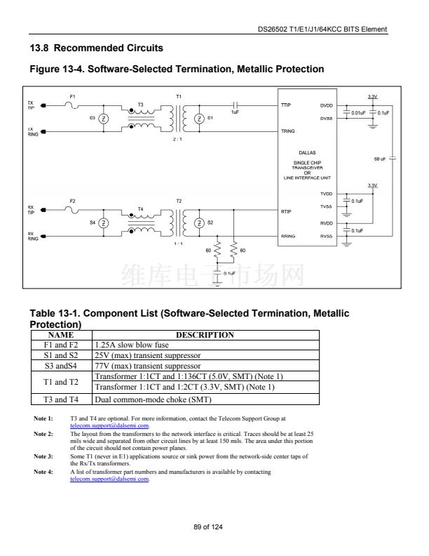
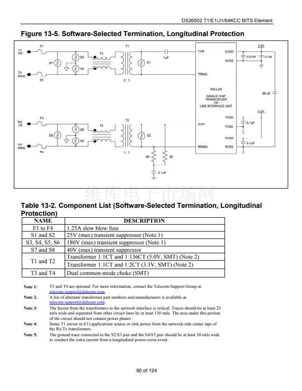
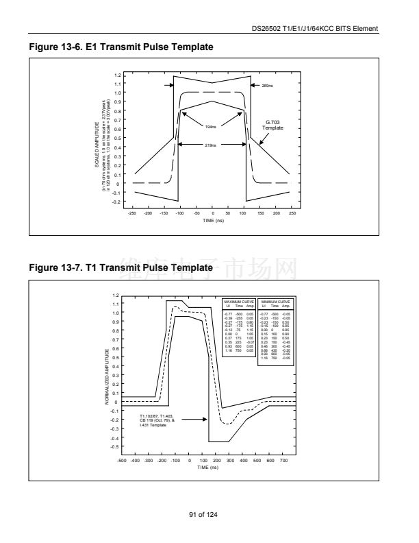
鈥?/div>
0
0
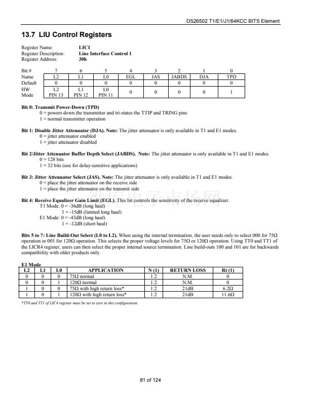
LIC2
Line Interface Control 2
31h
6
LIRST
0
0
5
IBPV
0
0
4
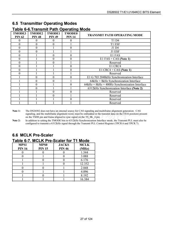
TAIS
0
TAIS
PIN 10
3
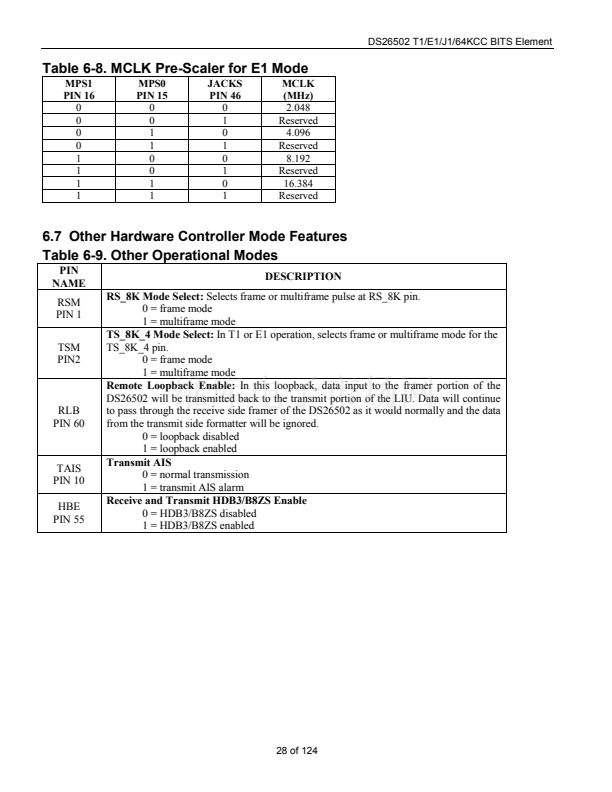
JACKS
0
JACKS
PIN 46
2
RCCFE
0
0
1
SCLD
0
0
0
CLDS
0
0
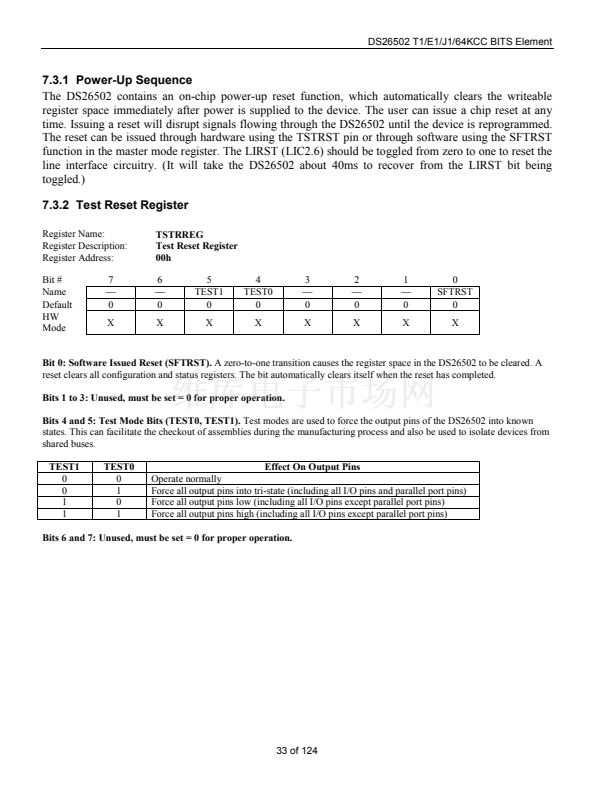
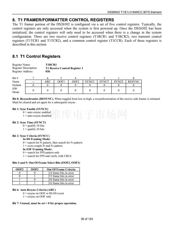
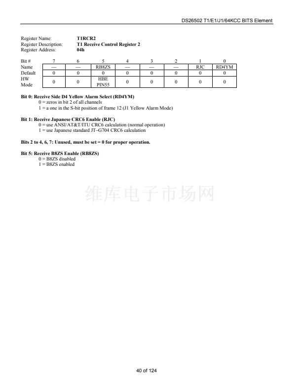
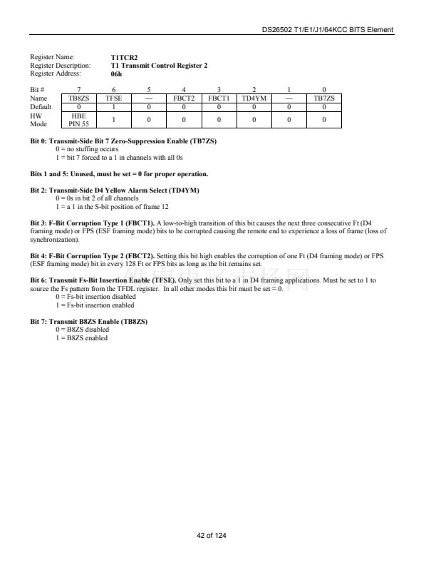
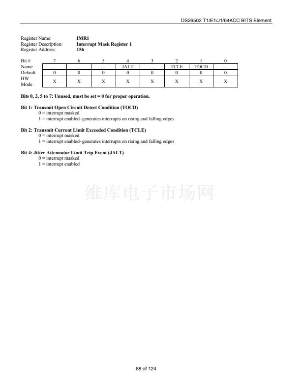
Bit 0: Custom Line Driver Select (CLDS).
Setting this bit to a one will redefine the operation of the transmit line driver.
When this bit is set to a one and LIC1.5 = LIC1.6 = LIC1.7 = 0, then the device will generate a square wave at the TTIP and
TRING outputs instead of a normal waveform. When this bit is set to a one and LIC1.5 = LIC1.6 = LIC1.7
鹿
0, then the device
will force TTIP and TRING outputs to become open-drain drivers instead of their normal push-pull operation. This bit should
be set to zero for normal operation of the device.
Note:
This bit should be set = 0 in 64KCC and 6312kHz transmit modes.
Bit 1: Short Circuit Limit Disable (in E1 mode) (SCLD).
Controls the 50mA (rms) current limiter.
Note:
Not applicable in
6312kHz mode.
0 = enable 50mA current limiter
1 = disable 50mA current limiter
Bit 2: Receive Composite Clock Filter Enable (RCCFE).
(64KCC mode only) Setting this bit will enable the PLL filter on
the received 64kHz composite clock.
Note:
the 8kHz and 400Hz output are not filtered.
0 = Receive Composite Clock Filter Disabled
1 = Receive Composite Clock Filter Enabled
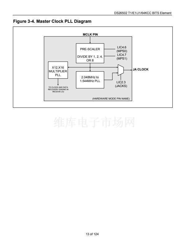
Bit 3: Jitter Attenuator Mux (JACKS).
Controls the source for JA CLOCK. This bit is only used in T1 mode.
0 = JA CLOCK sourced from the pre-scaled MCLK
1 = JA CLOCK sourced from internal PLL
Bit 4: Transmit Alarm Indication Signal (TAIS)
0 = transmit an unframed all-ones code
1 = transmit data normally
Bit 5: Insert BPV (IBPV).
A zero-to-one transition on this bit will cause a single BPV to be inserted into the transmit data
stream. Once this bit has been toggled from a zero to a one, the device waits for the next occurrence of three consecutive ones
to insert the BPV. This bit must be cleared and set again for a subsequent error to be inserted.
Note:
This function not
supported in 64KCC and 6312kHz modes.
Bit 6: Line Interface Reset (LIRST).
Setting this bit from a zero to a one will initiate an internal reset that resets the clock
recovery state machine and recenters the jitter attenuator. Normally this bit is only toggled on power-up. Must be cleared and
set again for a subsequent reset.
Bit 7: Unused, must be set = 0 for proper operation.
83 of 124


 1
1
 2
2
 3
3
 4
4
 5
5
 6
6
 7
7
 8
8
 9
9
 10
10
 11
11
 12
12
 13
13
 14
14
 15
15
 16
16
 17
17
 18
18
 19
19
 20
20
 21
21
 22
22
 23
23
 24
24
 25
25
 26
26
 27
27
 28
28
 29
29
 30
30
 31
31
 32
32
 33
33
 34
34
 35
35
 36
36
 37
37
 38
38
 39
39
 40
40
 41
41
 42
42
 43
43
 44
44
 45
45
 46
46
 47
47
 48
48
 49
49
 50
50
 51
51
 52
52
 53
53
 54
54
 55
55
 56
56
 57
57
 58
58
 59
59
 60
60
 61
61
 62
62
 63
63
 64
64
 65
65
 66
66
 67
67
 68
68
 69
69
 70
70
 71
71
 72
72
 73
73
 74
74
 75
75
 76
76
 77
77
 78
78
 79
79
 80
80
 81
81
 82
82
 83
83
 84
84
 85
85
 86
86
 87
87
 88
88
 89
89
 90
90
 91
91
 92
92
 93
93
 94
94
 95
95
 96
96
 97
97
 98
98
 99
99
 100
100
 101
101
 102
102
 103
103
 104
104
 105
105
 106
106
 107
107
 108
108
 109
109
 110
110
 111
111
 112
112
 113
113
 114
114
 115
115
 116
116
 117
117
 118
118
 119
119
 120
120
 121
121
 122
122
 123
123
 124
124
